ST STA508 40V 4.5A Quad Power Half Bridge Data Manual
Summary
The STA508 is a high-efficiency monolithic quad half bridge stage designed for professional digital audio amplification systems and stereo output stages. This comprehensive manual serves as a deep dive into the component's functionality, detailing key operational features like BCD Technology, thermal warning, and protection circuits. It covers complete pin descriptions, detailed electrical characteristics, and various configuration modes (single/dual/quad bridge). Essential for electronics engineers designing sophisticated, high-power audio equipment that requires reliable signal amplification.
Page 1 Text Content
STA508
40V 4.5A QUAD POWER HALF BRIDGE
FEATURES Figure 1. Package MULTIPOWER BCD TECHNOLOGY MINIMUM INPUT OUTPUT PULSE WIDTH DISTORTION
Power SO36
200mΩ Rds ON COMPLEMENTARY DMOS OUTPUT STAGE
Table 1. Order Codes
CMOS COMPATIBLE LOGIC INPUTS
Part Number Package
THERMAL PROTECTION
STA508 Power SO36
THERMAL WARNING OUTPUT UNDER VOLTAGE PROTECTION
The device is particularly designed to make the out- DESCRIPTION put stage of a stereo All-Digital High Efficiency (DDX™) amplifier capable to deliver 80 + 80W @
STA508 is a monolithic quad half bridge stage in Mul-
THD = 10% at Vcc 35V output power on 8Ω load.
tipower BCD Technology. The device can be used as
In single BTL configuration is also capable to deliver
dual bridge or reconfigured, by connecting CONFIG
a peak of 160W @THD = 10% at VCC = 35V on 4Ω
pin to Vdd pin, as single bridge with double current
load. The input pins have threshold proportional to VL
capability, and as half bridge (Binary mode) with half
pin voltage.
current capability.
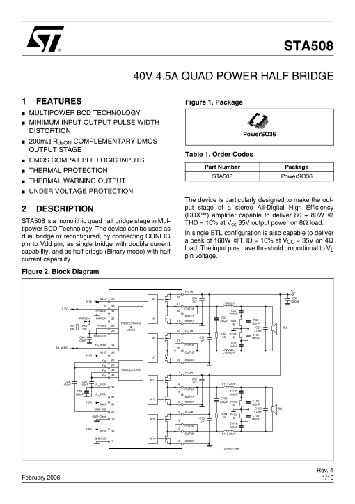
Figure 2. Block Diagram
VCC1A +VCC
IN1A M3 C30 C55 IN1A 1µF 1000µF
+3.3V OUT1A
CONFIG C20 100n F
OUT1A
PWRDNPWRDN M2 C52
GND1A 330p F R98 C99
PROTECTIONS 100n F
R57 R59 FAULT
10K 10K LOGIC
VCC1B 470n F
TRI-STATE
TH_WAR OUT1B 100n F
TH_WAR
IN1B OUT1B L19 22µH
VDD GND1B VDD VSS REGULATORS
VCC2A
100n F 100n F VCCSIGN L113 22µH
OUT2A
100n F VCCSIGN 100n F
OUT2A
IN2A GND2A 330p F R103 C107
IN2A 100n F
GND-Reg C108 8Ω
VCC2B 470n F
GND-Clean C106
OUT2B 100n F
OUT2B L112 22µH
GNDSUB M14
GND2B
D00AU1148B
Rev. 4
February 2006 1/10
Page Summary Contents For ST STA508 40V 4.5A Quad Power Half Bridge Data Manual
Manual Details
| Brand | QUAD |
|---|---|
| Pages | 10 |
| File Size | 174.10 KB |
| Published | June 04, 2026 |
Enter the captcha to get the download link:

Frequently Asked Questions
How much power can the device deliver on an 8Ω load?
It is capable to deliver 80 + 80W @ THD = 10% at V = 35V.
What are the thermal warning and fault indicator pins?
Pin 28 (TH-WAR) provides a Thermal Warning signal, and Pin 27 (FAULT) indicates if failure is detected.
Can this device be reconfigured for different power output modes?
Yes, it can operate in single BTL mode, dual bridge, or be reconfigured as a double current load with single bridge capability.
What specific protection features are available on the STA508?
The included protections are Thermal Protection, Thermal Warning Output, and Under Voltage Protection.