Page 1
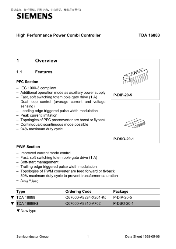
High Performance Power Combi Controller TDA Overview 1.1 Features PFC Section IEC 1000-3 compliant Additional operation mode as auxiliary power supply P-DIP-20-5 Fast, soft switching totem pole gate d...
Page 2
TDA 16888 Special Features High power factor Typical 50 µA start-up supply current Low quiescent current (15 m A) Undervoltage lockout with internal stand-by operation Internally synchronized fixed op...
Page 3
TDA 16888 P-DSO-20-1P-DIP-20-5 PFC IAC AUX VS PFC VS PFC CC PFC VC PFC IAC AUX VS PFC VS PFC CS PFC FB PFC CC PFC VC PFC CS PFC FB GND S ROSC GND S ROSC PFC CL PWM RMP PFC CL PWM RMP GND PWM IN GND PW...
Page 4
TDA 16888 1.3 Pin Definitions and Functions Pin No. Symbol Function PFC IAC AC line voltage sensing input VREF 7.5 V reference PFC CC PFC current loop compensation PFC CS PFC current sense GND Ground ...
Page 5
TDA 16888 PF PF PF AU ND PF PF PF PF IA FB VCPF CS VS CC VS CL CC UT 1.4 Block Diagram D3 TA D4 TA C2 Un de rv ol ta ge oc ko ut sc 7. FF Po we r M an ag em en RS Z2 Vo lta ge ef er en ce 7. (O ut pu ...
Page 6
TDA 16888 Functional Description Power Supply The TDA 16888 is protected against overvoltages typically above 17.5 V by an internal Zener diode Z3 at pin 9 (VCC) and against electrostatic discharging ...
Page 7
TDA 16888 Both PFC and PWM section are equipped with a peak current limitation, which is realized by the comparators C3 and C9 sensing at pin 6 (PFC CL) and pin 11 (PWM CS) respectively. When being ac...
Page 8
TDA 16888 PFC Section At normal operation the PFC section operates with dual loop control. An inner loop, which includes OP2, C1, FF1 and the PFC’s driver, controls the shape of the line current by av...
Page 9
TDA 16888 The pulse-width-modulation of the PWM section is trailing edge modulated according to the PWM ramp signal VPWM 15 (PWM RMP) and the input voltage VPWM RMP at pin IN at pin 14 (PWM IN) (see F...
Page 10
TDA 16888 Functional Block Description Gate Drive Both PFC and PWM section use fast totem pole gate drives at pin 8 (PFC OUT) and pin 10 (PWM OUT) respectively, which are designed to avoid cross condu...
Page 11
TDA 16888 The oscillator can be synchronized with an external clock signal supplied at pin (SYNC). As long as this clock signal is H the oscillator’s triangular signal VOSC is interrupted and its cloc...
Page 12
TDA 16888 Current Amplifier OP2 Being part of the inner loop the error amplifier OP2 controls the shape of the line current by comparison of the controlled current IQM with the measured average line c...
Page 13
TDA 16888 Comparator C1 The comparator C1 serves to adjust the duty cycle of the PFC gate drive. This is achieved by comparison of the output voltage of OP2 given at pin 3 (PFC CC) and the voltage ram...
Page 14
TDA 16888 Comparator C8 The control of the pulse width modulation of the PWM section is taken over by comparator C8 as soon as the soft start is finished. This is achieved by comparison of the PWM out...
Page 15
TDA 16888 Electrical Characteristics 4.1 Absolute Maximum Ratings TA = – 25 to 85 °C Parameter# Symbol Limit Values Unit Remarks min. max. VCC supply voltage VS 0.3 VZ3 VZ3 Zener voltage of Z3 Zener c...
Page 16
TDA 16888 4.1 Absolute Maximum Ratings (cont’d) TA = – 25 to 85 °C Parameter# Symbol Limit Values Unit Remarks min. max. Storage temperature TS °C Thermal resistance Rth JA K/W P-DIP-20-5 Thermal resi...
Page 17
TDA 16888 4.3 Characteristics Supply Section Parameter Symbol Limit Values Unit Test Condition min. typ. max. Zener voltage1) VZ3 16.0 17.5 19.0 IZ3 m A Zener current IZ3 µA VS 15.5 V2) Quiescent supp...
Page 18
TDA 16888 Undervoltage Lockout Parameter Symbol Limit Values Unit Test Condition min. typ. max. Power up, VS,UP 13.0 14.0 14.5 rising voltage threshold1) Power down, VS,DWN 10.5 11.0 11.5 falling volt...
Page 19
TDA 16888 External Voltage Reference Parameter Symbol Limit Values Unit Test Condition min. typ. max. Buffered output voltage VVREF 7.2 7.5 7.8 m A IVREF Line regulation ∆VVREF m V ∆VS Load regulation...
Page 20
TDA 16888 PFC Section Parameter Symbol Limit Values Unit Test Condition min. typ. max. Max duty cycle1) Don,PFC VPFC V3) OUT RROSC kΩ CL 4.7 n F Multiplier throttling VPFC 5.2 5.5 5.8 0.9 IPFC VS CS (...
Page 21
TDA 16888 Multiplier Parameter Symbol Limit Values Unit Test Condition min. typ. max. Input current IPFC m A IAC Input voltage VPFC 6.7 VC Exponential function, VPFC 1.1 VC threshold voltage Maximum o...
Page 22
TDA 16888 Operational Transconductance Amplifier (OTA1) Parameter Symbol Limit Values Unit Test Condition min. typ. max. Auxiliary power supply, VAUX 4.8 5.0 5.2 IPFC µA VS CS threshold voltage1) Mult...
Page 23
TDA 16888 Voltage Amplifier (OP1) Parameter Symbol Limit Values Unit Test Condition min. typ. max. Offset voltage VOff m V Input current IPFC µA VPFC FB FB Open loop gain APFC d B VC Input voltage ran...
Page 24
TDA 16888 Current Amplifier (OP2) Parameter Symbol Limit Values Unit Test Condition min. typ. max. Offset voltage VOff m V Input current IPFC n A CS IGND Open loop gain APFC d B CC Gain bandwidth prod...
Page 25
TDA 16888 PWM Section Parameter Symbol Limit Values Unit Test Condition min. typ. max. Undervoltage protection (C4), VPFC 3.8 4.0 4.2 VS threshold voltage Bias control (C5), VBC,Th 0.45 rising voltage...
Page 26
TDA 16888 Gate Drive (PWM and PFC Section) Parameter Symbol Limit Values Unit Test Condition min. typ. max. Output, minimum VOUT 1.2 VS voltage IOUT m A 1.5 VS IOUT m A 0.8 IOUT 1.6 2.0 IOUT m A 0.2 0...
Page 27
TDA 16888 Note: If not otherwise stated the figures shown in this section represent typical performance characteristics. AED02462 S, UPΙ VS, DWN VS, UP Figure 3 Undervoltage Lockout Hysteresis and Zen...
Page 28
TDA 16888 AED02464 kΩ ROSC Figure 5 PFC/PWM Frequency AED02465 on, PFC, max D kΩ ROSC Figure 6 Maximum PFC Duty Cycle Semiconductor Group Data Sheet 1998-05-06
Page 29
TDA 16888 AED02466 = 7 VVPFC VC PFC CCSΙ PFC IAC Figure 7 Multiplier Linearity AED02356 µA PFC CCSΙ PFC IACΙ VPFC VC Figure 8 Multiplier Dynamic Semiconductor Group Data Sheet 1998-05-06
Page 30
TDA 16888 AED02467 µA µA> 300 PFC IACΙ = 6 VVPFC VC PFC CCSΙ VPFC VS Figure 9 Multiplier Throttling by OTA2 AED02468 d B deg PFC VCA PFC VCAφ 10-2 10-1 Hz Frequency Figure 10 Open Loop Gain and Pha...
Page 31
TDA 16888 AED02469 φdegd B PFC CCA PFC CCAφ 10-2 10-1 Hz Frequency Figure 11 Open Loop Gain and Phase Characteristic of Current Amplifier OP2 AED02470 V1 PWM CSV PWM RMPV VPWMCS = 0 Figure 12 PWM Ramp...
Page 32
TDA 16888 AED02471 PFC OUTV Figure 13 Rising Edge of Driver Output AED02542 = 15 k Hzf OUT = 0.194 WPD0 Figure 14 Power Dissipation of Single Gate Driver at f OUT k Hz Semiconductor Group Data Sheet 1...
Page 33
TDA 16888 AED02543 m W DP = 1 = 50 k Hzf OUT = 0.197 WPD0 Figure 15 Power Dissipation of Single Gate Driver at f OUT k Hz AED02544 m W DP = 1 = 100 k Hzf OUT = 0.201 WPD0 Figure 16 Power Dissipation o...
Page 34
TDA 16888 AED02545 = 200 k Hzf OUT = 0.212 WPD0 Figure 17 Power Dissipation of Single Gate Driver at f OUT k Hz Semiconductor Group Data Sheet 1998-05-06
Page 35
TDA 16888 CLK OSC CLK OUT PFC RMPV VPFC CC PFC OUTV on, maxt PWM RMPV VPWM IN BC, Th V PWM OUTV on, maxt AET02546 Figure 18 Timing Diagram without Synchronization Semiconductor Group Data Sheet 1998-0...
Page 36
TDA 16888 OSCV SYNCV CLK OSC CLK OUT PFC RMPV VPFC CC PFC OUTV on, maxt PWM RMPV PWM INV VBC, Th PWM OUTV on, maxt AET02547 Figure 19 Timing Diagram with Synchronization (f SYNC > f OSC) Semiconduc...
Page 37
TDA 16888 OSCV SYNCV CLK OSC CLK OUT PFC RMPV PFC CCV PFC OUTV on, maxt PWM RMPV VPWM IN BC, Th V PWM OUTV on, maxt AET02548 Figure 20 Timing Diagram with Synchronization (f SYNC < f OSC) Semicondu...
Page 38
TDA 16888 Package Outlines P-DIP-20-5 (Plastic Dual In-line Package) Sorts of Packing Package outlines for tubes, trays etc. are contained in our Data Book “Package Information”. Dimensions in mm Semi...
Page 39
TDA 16888 P-DSO-20-1 (Plastic Dual Small Outline) 2. ax GPS05094 Index Marking 1) Does not include plastic or metal protrusions of 0.15 max per side 0. .0 2) Does not include dambar protrusion of 0.05...