# A B C D E F G H I J K L M N O P Q R S T U V W X Y Z

SIEMENS BTS 775 G User Guide

Summary

The BTS 775 G is a high-efficiency semiconductor module featuring quad switch drivers in a compact package. Utilizing ultra-low resistance technology and advanced SIEMENS SMART SIPMOS architecture, this device is optimized for robust DC motor management and H-Bridge configurations in critical applications. This technical guide provides a comprehensive overview of the BTS 775 G's specifications, block diagrams, pin definitions, and protection features (including short circuit and overtemperature detection). It is ideal for power electronics engineers designing high-performance solutions for automotive and industrial markets that demand maximized efficiency and reliability.
📄 Preview PAGE OF 17

Page 1 Text Content

Trilith IC BTS

Overview

Features Quad switch driver Free configurable as bridge or quad-switch Optimized for DC motor management applications

Ultra low RDS °C: ON @

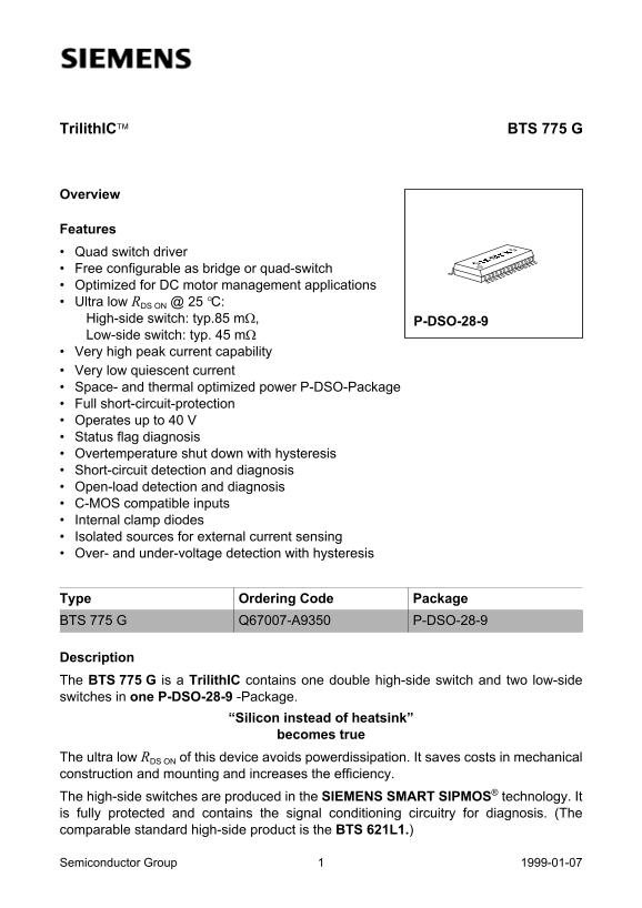
High-side switch: typ.85 mΩ, P-DSO-28-9 Low-side switch: typ. 45 mΩ Very high peak current capability Very low quiescent current Space- and thermal optimized power P-DSO-Package Full short-circuit-protection Operates up to 40 V Status flag diagnosis Overtemperature shut down with hysteresis Short-circuit detection and diagnosis Open-load detection and diagnosis C-MOS compatible inputs Internal clamp diodes Isolated sources for external current sensing Over- and under-voltage detection with hysteresis

Type Ordering Code Package BTS Q67007-A9350 P-DSO-28-9

Description The BTS G is a Trilith IC contains one double high-side switch and two low-side switches in one P-DSO-28-9 -Package.

“Silicon instead of heatsink” becomes true

The ultra low RDS

ON of this device avoids powerdissipation. It saves costs in mechanical

construction and mounting and increases the efficiency. The high-side switches are produced in the SIEMENS SMART SIPMOS® technology. It is fully protected and contains the signal conditioning circuitry for diagnosis. (The comparable standard high-side product is the BTS 621L1.)

Semiconductor Group 1999-01-07

Page Summary Contents For SIEMENS BTS 775 G User Guide

Page 1 Trilith IC BTS Overview Features Quad switch driver Free configurable as bridge or quad-switch Optimized for DC motor management applications Ultra low RDS °C: ON @ High-side switch: typ.85 mΩ, P-DSO...
Page 2 For minimized RDS ON the two low-side switches are N channel vertical power FETs in the SIEMENS SMART SIPMOS® technology. Fully protected by embedded protection functions. (The comparable standard pro...
Page 3 DL1 DL1 GL1 SL1 DL1 SL1 LS-Lead Frame 1 N.C. DL1 DHVS DHVS GND SH1 GH1 SH1 HS-Lead Frame ST SH2 GH2 SH2 DHVS DHVS N.C. DL2 DL2 LS-Lead Frame 2 SL2 GL2 SL2 DL2 DL2 AEP02071 Figure 1 Pin Configuration (...
Page 4 Pin Definitions and Functions Pin No. Symbol Function 1, 3, 25, 28 DL1 Drain of low-side switch1 Leadframe 1 GL1 Gate of low-side switch1 N.C. not connected 5, 10, 19, 24 DHVS Drain of high-side switc...
Page 5 Diagnosis Biasing and Protection Driver GH1 IN OUT LL00 HL10 O1 O2R 2120, SH2 GH2 HH11 1815,14,12, DL2 22, SH1 Protection DL1 Driver Protection Driver SL1 SL2 AEB02676 Figure 2 Block Diagram Semicondu...
Page 6 Circuit Description Input Circuit The control inputs GH1,2 consist of TTL/CMOS compatible Schmitt-Triggers with hysteresis. Buffer amplifiers are driven by these stages and convert the logic signal in...
Page 7 Overvoltage-Lockout (OVLO) When VS reaches the switch-off voltage VOVOFF the High-Side output transistors are switched off with a hysteresis. The IC becomes active if the supply voltage VS drops below...
Page 8 Truthtable and Diagnosis (valid only for the High-Side-Switches) Flag GH1 GH2 SH1 SH2 ST Remarks Inputs Outputs stand-by mode Normal operation; switch2 active identical with functional truth table swi...
Page 9 Electrical Characteristics Absolute Maximum Ratings – 40 °C < Tj < 150 °C Parameter Symbol Limit Values Unit Remarks min. max. High-Side-Switches (Pins DHVS, GH1,2 and SH1,2) Supply voltage VS –...
Page 10 Operating Range Parameter Symbol Limit Values Unit Remarks min. max. Supply voltage VS VUVOFF After VS rising above VUVON Input voltages VGH – 0.3 Input voltages VGL – 0.3 Output current IST m A HS-ju...
Page 11 Electrical Characteristics ISH1 = ISH2 = ISL1 = ISL2 = 0 A; – 40 °C < Tj < 150 °C; 8 V > VS > 18 V unless otherwise specified Parameter Symbol Limit Values Unit Test Condition min. typ. ma...
Page 12 Electrical Characteristics (cont’d) ISH1 = ISH2 = ISL1 = ISL2 = 0 A; – 40 °C < Tj < 150 °C; 8 V > VS > 18 V unless otherwise specified Parameter Symbol Limit Values Unit Test Condition min...
Page 13 Electrical Characteristics (cont’d) ISH1 = ISH2 = ISL1 = ISL2 = 0 A; – 40 °C < Tj < 150 °C; 8 V > VS > 18 V unless otherwise specified Parameter Symbol Limit Values Unit Test Condition min...
Page 14 Electrical Characteristics (cont’d) ISH1 = ISH2 = ISL1 = ISL2 = 0 A; – 40 °C < Tj < 150 °C; 8 V > VS > 18 V unless otherwise specified Parameter Symbol Limit Values Unit Test Condition min...
Page 15 SΙ = 12 V SV CS CL FH1, 470n F F100 ST 5, 10, 19, 24 Diagnosis Biasing and Protection VDSH1 DSH2V FL1V--VFL2 Driver IN OUT STV VSTL LL00 HL10 O2R SH2Ι STZV SH2 VGH1 HH11 12, 14, 15, 18 DL2 DL2Ι VUVON ...
Page 16 Watchdog Reset TLE 4278G DO1 1N4001 RQ CQ CD CS WD DHVS ST 5, 10, 19, 24 Diagnosis Biasing and Protection Driver IN OUT HL10 O2R 12, 14, 15, 18 DL2 22, 23 SH1 1, 3, DL1 Protection GL1 Gate Driver Prot...
Page 17 Package Outlines P-DSO-28-9 (Plastic Dual Small Outline Package) 2. ax Index Marking 1) Does not include plastic or metal protrusions of 0.15 max rer side 2) Does not include dambar protrusion of 0.05...

Manual Details

Brand Siemens
Pages 17
File Size 110.74 KB
Published June 04, 2026
44 views

Enter the captcha to get the download link:

captcha

Frequently Asked Questions

What operating configurations is the BTS 775 G suitable for?

It can operate in H-Bridge configuration, or as a bridge or quad-switch by connecting its separate power transistor sources to different pins.

What safety protections are built into the output stages?

The outputs feature full short-circuit protection against ground and supply voltage shorts. Additionally, it includes overtemperature shutdown with hysteresis.

How does this device improve efficiency compared to traditional designs?

Its ultra low Resistance (R) minimizes power dissipation, achieving 'Silicon instead of heatsink' by saving costs on mechanical construction.

Are the control inputs compatible with standard microcontroller signals?

Yes, the GH1 and GH2 control inputs are TTL/CMOS compatible Schmitt-Triggers with hysteresis for reliable signal processing.