# A B C D E F G H I J K L M N O P Q R S T U V W X Y Z

SIEMENS TLE 4262 User Guide

Summary

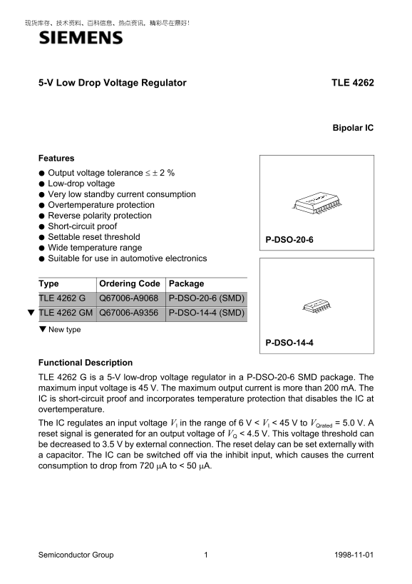
The TLE 4262 is a robust 5V, low-drop voltage regulator IC designed for reliable power stabilization in demanding applications, including automotive electronics. This manual provides comprehensive technical documentation detailing its operation, covering key features such as ultra-low standby current, short-circuit protection, and adjustable reset thresholds. Engineers can use this resource to understand the circuit architecture, view detailed electrical characteristics curves (including input/output response), and utilize precise packaging specifications for integration into modern electronic designs.
📄 Preview PAGE OF 15

Page 1 Text Content

5-V Low Drop Voltage Regulator TLE

Bipolar IC

Features Output voltage tolerance ≤ ± 2 % Low-drop voltage Very low standby current consumption Overtemperature protection Reverse polarity protection Short-circuit proof Settable reset threshold

P-DSO-20-6

Wide temperature range Suitable for use in automotive electronics

Type Ordering Code Package TLE 4262 G Q67006-A9068 P-DSO-20-6 (SMD) TLE 4262 GM Q67006-A9356 P-DSO-14-4 (SMD) ▼ New type

P-DSO-14-4

Functional Description TLE 4262 G is a 5-V low-drop voltage regulator in a P-DSO-20-6 SMD package. The maximum input voltage is 45 V. The maximum output current is more than 200 m A. The IC is short-circuit proof and incorporates temperature protection that disables the IC at overtemperature.

The IC regulates an input voltage VI in the range of 6 V < VI < 45 V to VQrated = 5.0 V. A reset signal is generated for an output voltage of VQ < 4.5 V. This voltage threshold can

be decreased to 3.5 V by external connection. The reset delay can be set externally with a capacitor. The IC can be switched off via the inhibit input, which causes the current consumption to drop from 720 µA to < µA.

Semiconductor Group 1998-11-01

Page Summary Contents For SIEMENS TLE 4262 User Guide

Page 1 5-V Low Drop Voltage Regulator TLE Bipolar IC Features Output voltage tolerance ≤ ± 2 % Low-drop voltage Very low standby current consumption Overtemperature protection Reverse polarity protection Sho...
Page 2 Dimensioning Information on External Components The input capacitor CI is necessary for compensating line influences. Using a resistor of approx. 1 Ω in series with CI, the oscillating circuit consist...
Page 3 Pin Definitions and Functions Pin Symbol Function INH Inhibit; TTL-compatible, low-active input QRES Reset output; open-collector output internally connected to the output via a resistor of 30 kΩ. 4-7...
Page 4 Circuit Description The control amplifier compares a reference voltage, which is kept highly accurate by resistance adjustment, to a voltage that is proportional to the output voltage and drives the b...
Page 5 Absolute Maximum Ratings Parameter Symbol Limit Values Unit Remarks min. max. Input Input voltage VI Input current II internally limited Reset Output Voltage VR – 0.3 Current IR internally limited Res...
Page 6 Absolute Maximum Ratings (cont’d) Parameter Symbol Limit Values Unit Remarks min. max. Temperature Junction temperature Tj °C Storage temperature Tstg °C Operating Range Input voltage VI 5.2 Junction ...
Page 7 Characteristics VI = 13.5 V; Tj = 25 °C; Ve &gt; 3.5 V; (unless specified otherwise) Parameter Symbol Limit Values Unit Test Condition min. typ. max. Normal Operation Output voltage VQ 4.9 5.00 5.10 5...
Page 8 Characteristics (cont’d) VI = 13.5 V; Tj = 25 °C; Ve &gt; 3.5 V; (unless specified otherwise) Parameter Symbol Limit Values Unit Test Condition min. typ. max. Saturation voltage VC m V VQ &lt; VRT Cha...
Page 9 Input Output TLE 4262G Reset to MC AES01084 Application Circuit TLE 4262G 5.6 k r+Ι QV cd GND Dr ΙV SVR = 20 log *) Below Regulating Range AES01082 Test Circuit Semiconductor Group 1998-11-01
Page 10 RTV QV d TV cd V STV td Power-on-Reset Over- Voltage Drop Undervoltage Secondary Load temperature at Input Spike Bounce AET01085 Time Response Semiconductor Group 1998-11-01
Page 11 TLE 4262 G Charge Current versus Switching Voltage Vd T and VST Temperature versus Temperature AED01086 AED01087 ,d TV cd = 13.5 V = 1.5 V cd Reset Switching Threshold Current Consumption of Inhibit v...
Page 12 TLE 4262 G Output Voltage versus Output Current versus Temperature Input Voltage AED01090 AED01091 VQ = 25 Cj = 13.5 Ve Input Response Load Response AED01092 AED01093 µ1 s=t m A ft m V m V QV Semicond...
Page 13 Drop Voltage versus Current Consumption versus Output Current Output Current AED01094 AED01095 m V m A Dr V Current Consumption versus Output Voltage versus Input Voltage Input Voltage AED01096 AED010...
Page 14 Package Outlines P-DSO-20-6 (Plastic Dual Small Outline) 2. ax GPS05094 Index Marking .0 8˚ ax+0 1) Does not include plastic or metal protrusions of 0.15 max per side 2) Does not include dambar protru...
Page 15 P-DSO-14-4 (Plastic Dual Small Outline) 1. ax Index Marking 1) Does not include plastic or metal protrusion of 0.15 max. per side 2) Does not include dambar protrusion of 0.05 max. per side GPS05093 8...

Manual Details

Brand Siemens
Pages 15
File Size 151.96 KB
Published June 02, 2026
59 views

Enter the captcha to get the download link:

captcha

Frequently Asked Questions

What input and output capacitors are required for stable operation?

An input capacitor C requires a series resistor (approx. 1W), and the output capacitor must be at least 22mF with an ESR of no more than 3Ω.

Are there built-in protective features on this IC?

Yes, it includes overtemperature protection, reverse polarity protection, short-circuit proof capability, and low-drop voltage regulation.

How can I adjust the reset signal threshold?

The reset threshold (SRES) can be adjusted by connecting a voltage divider from the output to ground at Pin 10.

What is the standard operating input voltage range?

The regulator operates on an input voltage V in the range of 6 V to 45 V, and targets a regulated output of 5.0 V.