Siemens CGY31 User Guide
Summary
This high-performance GaAs MMIC amplifier is a two-stage monolithic microwave integrated circuit designed for reliable RF signal amplification across a wide frequency spectrum. The comprehensive manual provides RF engineers and designers with essential technical documentation, including maximum ratings, detailed electrical characteristics, S parameters, application circuits, and crucial guidelines for optimal operation. Use this resource to ensure proper handling (ESD precautions) and integration of the amplifier into your high-frequency microwave systems while achieving guaranteed performance metrics like gain flatness and low noise figure.
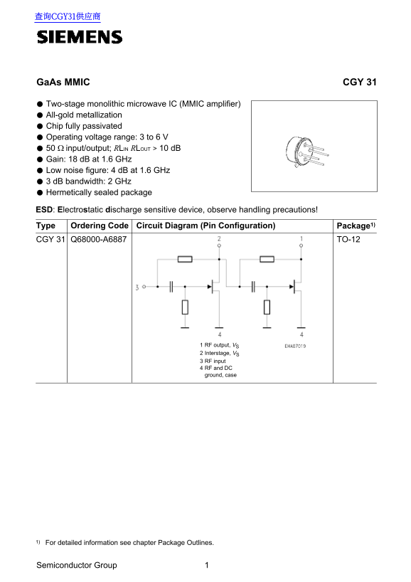
Page 1 Text Content
查询CGY31供应商
Ga As MMIC CGY 31
Two-stage monolithic microwave IC (MMIC amplifier) All-gold metallization Chip fully passivated Operating voltage range: 3 to 6 input/output; RLIN RLOUT > 10 d B Gain: 18 d B at 1.6 GHz Low noise figure: 4 d B at 1.6 GHz d B bandwidth: 2 GHz Hermetically sealed package
ESD: Electrostatic discharge sensitive device, observe handling precautions! Type Ordering Code Package1)Circuit Diagram (Pin Configuration) CGY 31 Q68000-A6887 TO-12
RF output, VS Interstage, VS RF input RF and DC ground, case
1) For detailed information see chapter Package Outlines.
Semiconductor Group
Page Summary Contents For Siemens CGY31 User Guide
Manual Details
| Brand | Siemens |
|---|---|
| Pages | 9 |
| File Size | 132.84 KB |
| Published | May 29, 2026 |
Enter the captcha to get the download link:

Frequently Asked Questions
What is the required handling for this MMIC device?
It is ESD sensitive; observe handling precautions to protect against degradation due to excess voltage or excess current spikes.
What ground connection setup ensures stable operation?
An excellent ground connection of lead 4 and package (e.g., soldered on microstripline laminate) is required, providing adequate heat sink.
Are DC isolation methods necessary for connections?
Yes, input and output connections must be DC isolated by coupling capacitors.
What are the device's performance characteristics at 1.6 GHz (typical)?
It offers a gain of 18 dB, a low noise figure of 4 dB, and a 3 dB bandwidth of 2 GHz.