SIEMENS Silicon N-Channel MOSFET Tetrode BF 996 S Data Sheet User Manual
Summary
This comprehensive datasheet provides the full technical specifications for the BF996S Silicon N Channel MOSFET Tetrode, an advanced component designed for signal amplification in UHF TV tuner input stages. Engineers will find critical operational details covering maximum ratings, deep dive DC/AC characteristics, power gain measurements (up to 800 MHz), and reliable low noise figure performance. This resource is essential for R&D teams and circuit designers requiring precision components with high transconductance for professional RF electronics applications.
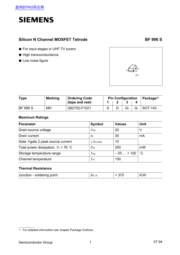
Page 1 Text Content
查询BF996S供应商
Silicon N Channel MOSFET Tetrode BF 996 S
For input stages in UHF TV tuners High transconductance Low noise figure
Type Marking Ordering Code Package1)Pin Configuration (tape and reel)
BF 996 S Q62702-F1021MH G2 G1 SOT-143
Maximum Ratings
Parameter Symbol Values Unit Drain-source voltage VDS
ID m ADrain current Gate 1/gate 2 peak source current IG1/2SM
Total power dissipation, TA < 76 ˚C Ptot m W
Storage temperature range Tstg – 55 … + 150 ˚C
Channel temperature Tch
Thermal Resistance
Junction - soldering point Rth JS K/W
1) For detailed information see chapter Package Outlines.
Semiconductor Group 07.94
Page Summary Contents For SIEMENS Silicon N-Channel MOSFET Tetrode BF 996 S Data Sheet User Manual
Manual Details
| Brand | Siemens |
|---|---|
| Pages | 8 |
| File Size | 140.23 KB |
| Published | June 01, 2026 |
Enter the captcha to get the download link:

Frequently Asked Questions
What is the maximum recommended channel temperature?
The channel temperature ($T_{ch}$) must not exceed 150°C.
How high must the junction-to-soldering point thermal resistance be avoided?
The thermal resistance $R_{thJS}$ should be less than 370 K/W.
What is the typical forward transconductance ($g_{fs}$) value?
At $V_{DS}=15$ V and $I_D=10$ mA, the typical transconductance is 18 mS.
What voltage range determines the gate source breakdown voltages?
Both Gate 1 and Gate 2 have a breakdown voltage ($V(BR)$) that ranges from 8.5 V to 14 V.