Siemens HITFET BTS 941 Smart Lowside Power Switch User Manual and Specification Sheet
Summary
This comprehensive manual details the HITFET BTS 941 Smart Lowside Power Switch, a robust component designed for switching various loads in DC applications (e.g., 12V and 24V). It provides detailed electrical specifications regarding drain source voltage, on-state resistance, and multiple integrated protection features, including thermal shutdown, overcurrent, and short circuit protection. Essential for electronics designers and engineers building reliable power control circuits, this document guides the proper implementation of solid-state relay alternatives that replace electromechanical relays.
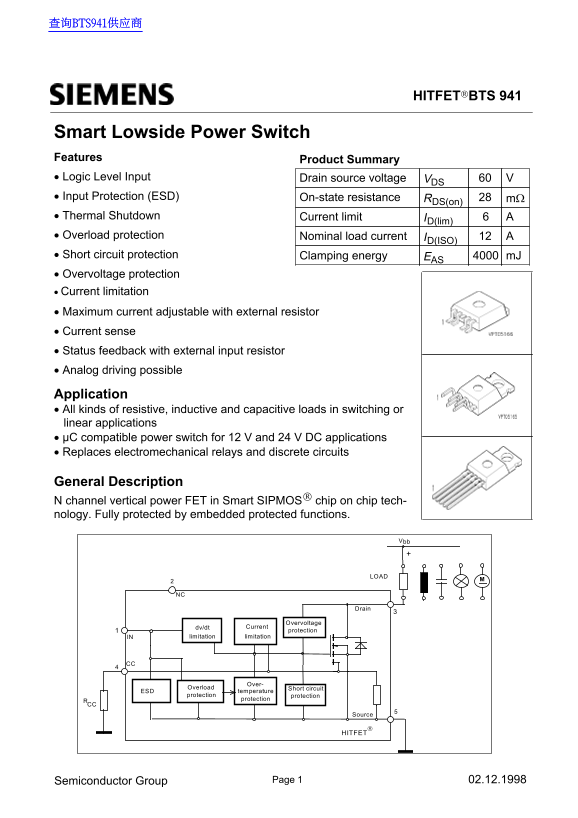
Page 1 Text Content
查询BTS941供应商
HITFETBTS 941
Smart Lowside Power Switch Features Product Summary • Logic Level Input Drain source voltage V60VDS • Input Protection (ESD) On-state resistance RDS(on) mΩ • Thermal Shutdown ID(lim) ACurrent limit • Overload protection Nominal load current AID(ISO) • Short circuit protection Clamping energy m JEAS • Overvoltage protection • Current limitation • Maximum current adjustable with external resistor • Current sense • Status feedback with external input resistor • Analog driving possible
Application • All kinds of resistive, inductive and capacitive loads in switching or linear applications • µC compatible power switch for 12 V and 24 V DC applications • Replaces electromechanical relays and discrete circuits
General Description N channel vertical power FET in Smart SIPMOS chip on chip tech- nology. Fully protected by embedded protected functions.
Drain
Overvoltage
dv/dt Current
protection
IN limitation limitation
Over-
Overload
ESD temperature Short circuit
protection
protection protection
Source
HITFET
02.12.1998Semiconductor Group
Page Summary Contents For Siemens HITFET BTS 941 Smart Lowside Power Switch User Manual and Specification Sheet
Manual Details
| Brand | Siemens |
|---|---|
| Pages | 11 |
| File Size | 180.23 KB |
| Published | May 31, 2026 |
Enter the captcha to get the download link:

Frequently Asked Questions
What is the maximum single pulse inductive energy this device can handle?
The Unclamped single pulse inductive energy (EAS) rating is 4000 mJ.
What voltage ranges is this power switch designed to operate with?
It is a compatible power switch for both 12 V and 24 V DC applications.
What materials or types of loads can the BTS941 efficiently manage?
It is suitable for all kinds of resistive, inductive, and capacitive loads in switching or linear applications.
How does the device prevent overheating during operation?
It features thermal shutdown protection with a required trip temperature range of 150–165°C.