Siemens BGA 425 Data Handbook
Summary
This high-performance BGA 425 Si-MMIC-Amplifier is a multifunctional integrated circuit designed for advanced RF signal processing applications, including Low Noise Amplifiers (LNA) and Mixers. The supporting manual provides comprehensive electrical characteristics, detailing critical operational parameters such as insertion gain, noise figure, and reverse isolation across multiple frequencies (up to 10 GHz). It serves electronics engineers who require precise components for complex RF circuit design and integration.
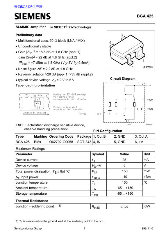
Page 1 Text Content
查询BGA425供应商
BGA 425
Si-MMIC-Amplifier in SIEGET 25-Technologie
3Preliminary data
• Multifunctional casc. 50 Ω block (LNA / MIX) • Unconditionally stable • Gain |S21|2 = 18.5 d B at 1.8 GHz (appl.1) gain |S21|2 = 22 d B at 1.8 GHz (appl.2) IP3out = +7 d Bm at 1.8 GHz (VD=3V,ID=9.5m A)
VPS05605
• Noise figure NF = 2.2 d B at 1.8 GHz • Reverse isolation >28 d B (appl.1) >35 d B (appl.2)
Circuit Diagram
• typical device voltage VD = 2 V to 5 V Tape loading orientation
GNDESD: Electrostatic discharge sensitive device, EHA07371
observe handling precaution!
PIN Configuration
Type Marking Ordering Code 1, Out B 3, Out A2, GNDPackage BGA 425 Q62702-G0058 SOT-343 4, IN 5, GND 6, +VBMs
Maximum Ratings
Parameter Symbol Value Unit
Device current ID m A Device voltage VD,+V V6
Total power dissipation, TS ≤ tbd °C Ptot m W
RF input power PRFin -10 d Bm
Junction temperature Tj °C Ambient temperature TA -65 ...+150 Storage temperature Tstg -65 ...+150
Thermal Resistance
Junction - soldering point 1) Rth JS ≤ tbd K/W
1) TS is measured on the ground lead at the soldering point to the pcb Semiconductor Group Jul-14-19981 Semiconductor Group 1998-11-01
Page Summary Contents For Siemens BGA 425 Data Handbook
Manual Details
| Brand | Siemens |
|---|---|
| Pages | 8 |
| File Size | 84.11 KB |
| Published | June 06, 2026 |
Enter the captcha to get the download link:

Frequently Asked Questions
How should I handle this device?
Be aware that this is an ESD sensitive device; you must observe general handling precautions.
What board design features are critical for installation?
Connection of large-value capacitors from pin 6 to ground near the device is essential. Also, use plated through holes at pins 2 and 5 on thin boards.
What are the primary electrical performance metrics at 1.8 GHz?
Typical gain $|S_{12}|$ is 18.5 dB, and the intercept point (IP) is +7 dBm when operating at V=3V and I=9.5mA.