ROHM US6M2 User Guide
Summary
This is the technical datasheet for the ROHM US6M2 dual N-channel and P-channel MOSFET transistor. It features 2.5V gate drive capability, high-speed switching, and low on-resistance in a compact TUMT6 package. The N-channel MOSFET supports 30V drain-source voltage with ±1.5A continuous drain current, while the P-channel supports -20V with ±1A current. Built-in G-S protection diode and ESD protection are included. Target applications include switching circuits in portable electronics. Target users are electronics design engineers and circuit designers requiring low-voltage driven complementary MOSFET pairs for space-constrained applications.
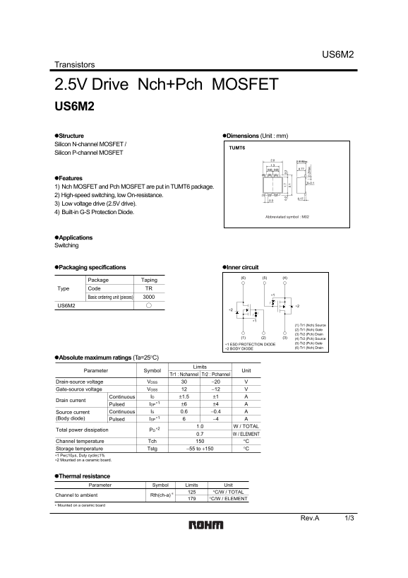
Page 1 Text Content
US6M2
Transistors
2.5V Drive Nch+Pch MOSFET US6M2 Structure Dimensions (Unit : mm) Silicon N-channel MOSFET /
TUMT6
Silicon P-channel MOSFET
Features 1) Nch MOSFET and Pch MOSFET are put in TUMT6 package. 2) High-speed switching, low On-resistance. 3) Low voltage drive (2.5V drive). 4) Built-in G-S Protection Diode.
Abbreviated symbol : M02
Applications Switching
Packaging specifications Inner circuit
Package Taping
Type Code TR
Basic ordering unit (pieces)
US6M2 ∗2
∗2 0. 2M ax
(1) Tr1 (Nch) Source (2) Tr1 (Nch) Gate (3) Tr2 (Pch) Drain
(1) (2) (3) (4) Tr2 (Pch) Source
∗1 ESD PROTECTION DIODE (5) Tr2 (Pch) Gate ∗2 BODY DIODE (6) Tr1 (Nch) Drain
Absolute maximum ratings (Ta=25°C)
Limits
Parameter Symbol Unit
Tr1 : Nchannel Tr2 : Pchannel
Drain-source voltage VDSS −20 V30 Gate-source voltage VGSS −12 Continuous ID ±1.5 ±1
Drain current
∗1 Pulsed IDP ±6 ±4 Continuous Source current IS 0.6 −0.4 (Body diode) ∗1 Pulsed ISP −4
1.0 W / TOTAL∗2
Total power dissipation PD
W / ELEMENT0.7
Channel temperature °CTch
Storage temperature −55 to +150 °CTstg
∗1 Pw≤10µs, Duty cycle≤1% ∗2 Mounted on a ceramic board.
Thermal resistance
Parameter Symbol Limits Unit
°C/W / TOTAL
Channel to ambient Rth(ch-a)
°C/W / ELEMENT179
∗ Mounted on a ceramic board
Rev.A 1/3
Page Summary Contents For ROHM US6M2 User Guide
Manual Details
| Brand | ROHM |
|---|---|
| Pages | 4 |
| File Size | 69.62 KB |
| Published | June 16, 2026 |
Enter the captcha to get the download link:

Frequently Asked Questions
What is the maximum drain current for the N-channel MOSFET?
Continuous drain current is 1.5A, with pulsed current up to 6A.
What is the typical on-resistance for the P-channel MOSFET?
Typical RDS(on) is 280 mΩ at ID=-1A, VGS=-4.5V.
What is the gate-source voltage rating?
The absolute maximum rating for gate-source voltage is ±12V.
Can this device be used in medical or aerospace applications?
No, it's for ordinary electronic equipment; consult ROHM for safety-critical applications.