ROHM TT8U2 Product Specification Sheet
Summary
This essential technical manual details the TSST8 MOSFET/Schottky diode combo chip, designed for high-efficiency switching applications. Featuring low on-resistance, built-in body diodes, and excellent thermal performance, this component is ideal for engineers integrating robust power control into electronic appliances or communication devices. The documentation provides comprehensive absolute maximum ratings, electrical characteristics, and application guidelines to ensure correct circuit design and reliable system operation.
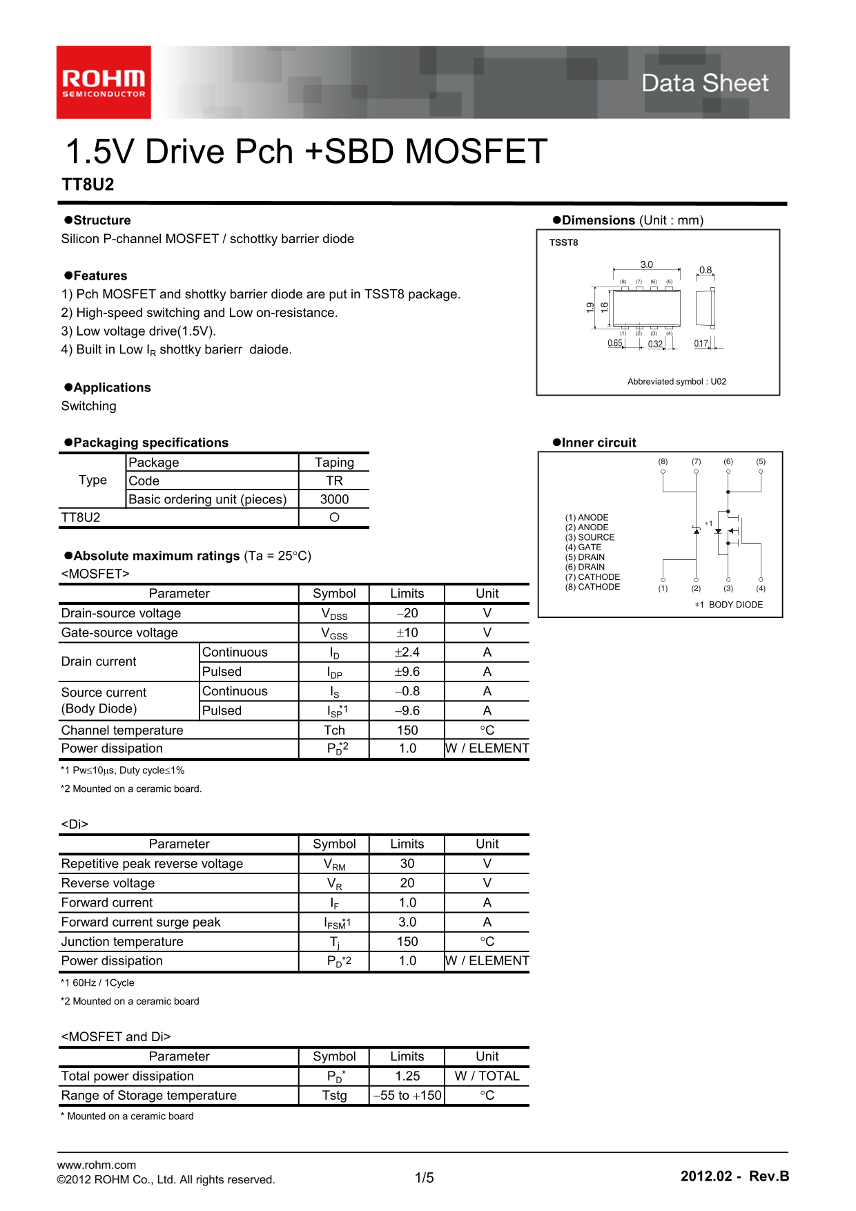
Page 1 Text Content
1.5V Drive Pch +SBD MOSFET TT8U2 Structure Dimensions (Unit : mm) Silicon P-channel MOSFET / schottky barrier diode TSST8
Features
1) Pch MOSFET and shottky barrier diode are put in TSST8 package. 2) High-speed switching and Low on-resistance.
3) Low voltage drive(1.5V). (1) (2) (3) (4)
4) Built in Low IR shottky barierr daiode.
Abbreviated symbol : U02
Applications Switching
Packaging specifications Inner circuit
Package Taping (8) (7) (6) (5)
Type Code TR
Basic ordering unit (pieces)
TT8U2 (1) ANODE
(2) ANODE (3) SOURCE (4) GATE Absolute maximum ratings (Ta = 25C) (5) DRAIN (6) DRAIN
<MOSFET> (7) CATHODE
(8) CATHODE (1) (2) (3) (4)
Parameter Symbol Limits Unit
∗1 BODY DIODE
Drain-source voltage VDSS 20 Gate-source voltage VGSS 10 Continuous ID 2.4
Drain current
Pulsed IDP 9.6 Source current Continuous IS 0.8
(Body Diode) Pulsed ISP *1 9.6
Channel temperature Tch C
Power dissipation PD 1.0 W / ELEMENT
*1 Pw10s, Duty cycle1%
*2 Mounted on a ceramic board.
Parameter Symbol Limits Unit
Repetitive peak reverse voltage VRM Reverse voltage VR
Forward current IF 1.0
Forward current surge peak IFSM *1 3.0
Junction temperature Tj C
Power dissipation PD *2 1.0 W / ELEMENT
*1 60Hz / 1Cycle
*2 Mounted on a ceramic board
<MOSFET and Di>
Parameter Symbol Limits Unit
Total power dissipation PD 1.25 W / TOTAL
Range of Storage temperature Tstg 55 to 150 C * Mounted on a ceramic board
www.rohm.com
©2012 ROHM Co., Ltd. All rights reserved. 1/5 2012.02 - Rev.B
Page Summary Contents For ROHM TT8U2 Product Specification Sheet
Manual Details
| Brand | ROHM |
|---|---|
| Pages | 6 |
| File Size | 475.31 KB |
| Published | July 22, 2026 |
Enter the captcha to get the download link:

Frequently Asked Questions
What is the maximum drain-source voltage ($V_{DSS}$) this device can handle?
The absolute maximum rating for the Drain-source voltage ($V_{DSS}$) is -20 V.
Can this component be used in critical life support systems, like medical instruments?
No. It's not designed for equipment requiring an extremely high level of reliability or those posing a direct threat to human life.
What are the key electrical features of this MOSFET package?
It features low-voltage drive (1.5V) and includes a built-in low I Schottky barrier diode.
Where must the device be mounted to ensure proper power dissipation?
The datasheet repeatedly advises that components should be mounted on a ceramic board.