ROHM IMX25 Product Specification Manual
Summary
This dual isolated transistor module offers a cost-effective and space-saving solution by packaging two independent NPN transistors in one SMT unit. Designed for general-purpose electronic applications, including communication devices, office automation, and appliances, this component ensures reliable performance where element independence is crucial. The manual provides extensive technical documentation, covering absolute maximum ratings, detailed electrical specifications (like breakdown voltages and saturation curves), thermal characteristics, and packaging guidelines necessary for precise circuit design optimization.
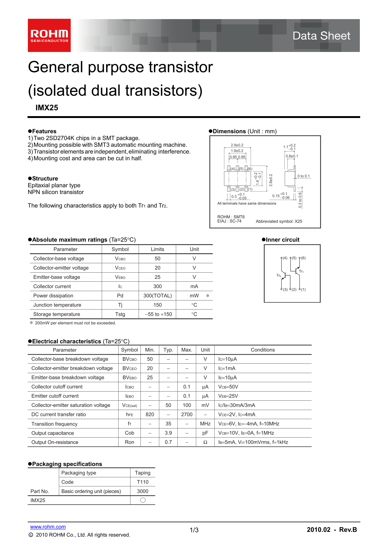
Page 1 Text Content
General purpose transistor (isolated dual transistors) IMX25 Features Dimensions (Unit : mm) 1) Two 2SD2704K chips in a SMT package.
2) Mounting possible with SMT3 automatic mounting machine. 2.9±0.2
3) Transistor elements are independent, eliminating interference.
4) Mounting cost and area can be cut in half.
0 to 0.1
Structure Epitaxial planar type
NPN silicon transistor +0.1
All terminals have same dimensions
The following characteristics apply to both Tr1 and Tr2.
ROHM : SMT6 EIAJ : SC-74 Abbreviated symbol: X25
Absolute maximum ratings (Ta=25C) Inner circuit
Parameter Symbol Limits Unit
Collector-base voltage VCBO −0 .1
Collector-emitter voltage VCEO
Tr1 2. 8± 0.
Emitter-base voltage VEBO
Collector current IC m A
Power dissipation Pd 300(TOTAL) m W
0. to .60.15
Junction temperature Tj °C
Storage temperature Tstg −55 to +150 °C
∗ 200m W per element must not be exceeded.
Electrical characteristics (Ta=25C)
Parameter Symbol Min. Typ. Max. Unit Conditions
Collector-base breakdown voltage BVCBO IC=10μA
Collector-emitter breakdown voltage BVCEO IC=1m A
Emitter-base breakdown voltage BVEBO IE=10μA
Collector cutoff current ICBO 0.1 μA VCB=50V
Emitter cutoff current IEBO 0.1 μA VEB=25V
Collector-emitter saturation voltage VCE(sat) m V IC/IB=30m A/3m A
DC current transfer ratio h FE VCE=2V, IC=4m A
Transition frequency f T MHz VCE=6V, IE=−4m A, f=10MHz
Output capacitance Cob 3.9 p F VCB=10V, IE=0A, f=1MHz
Output On-resistance Ron 0.7 IB=5m A, Vi=100m Vrms, f=1k Hz
Packaging specifications
Packaging type Taping
Code T110
Part No. Basic ordering unit (pieces)
IMX25
www.rohm.com
1/3 2010.02 - Rev.B
○c 2010 ROHM Co., Ltd. All rights reserved.
Page Summary Contents For ROHM IMX25 Product Specification Manual
Manual Details
| Brand | ROHM |
|---|---|
| Pages | 4 |
| File Size | 139.75 KB |
| Published | July 15, 2026 |
Enter the captcha to get the download link:

Frequently Asked Questions
Can I use this transistor for life support or critical safety systems?
No, this product is not designed for equipment requiring an extremely high level of reliability, such as medical instruments or aerospace machinery.
What general electronics applications are these components meant for?
They are intended for use with general-use electronic equipment like audio visual, office-automation, communication devices, and amusement appliances.
What is the maximum allowable total power dissipation?
The total recommended power dissipation ($P_d$) is 300 mW, but per element, it must not exceed 200 mW.
In terms of unique features, what does this structure offer over standard designs?
Because the transistor elements are independent, they eliminate signal interference and can help reduce mounting cost and area.