ROHM SH8M11 User Guide
Summary
Boost your power switching performance with the SH8M11 N-channel/P-channel MOSFET. Engineered for efficiency and reliability in demanding applications, this device features low on-resistance and a robust SOP8 package suitable for various power circuits. This comprehensive manual serves as the engineer's definitive guide, providing exhaustive technical data including electrical characteristics, absolute maximum ratings, transient thermal analysis, and detailed measurement circuit guides. It is designed specifically for power electronics designers who require precise specifications to optimize switching efficiency and ensure reliable system operation.
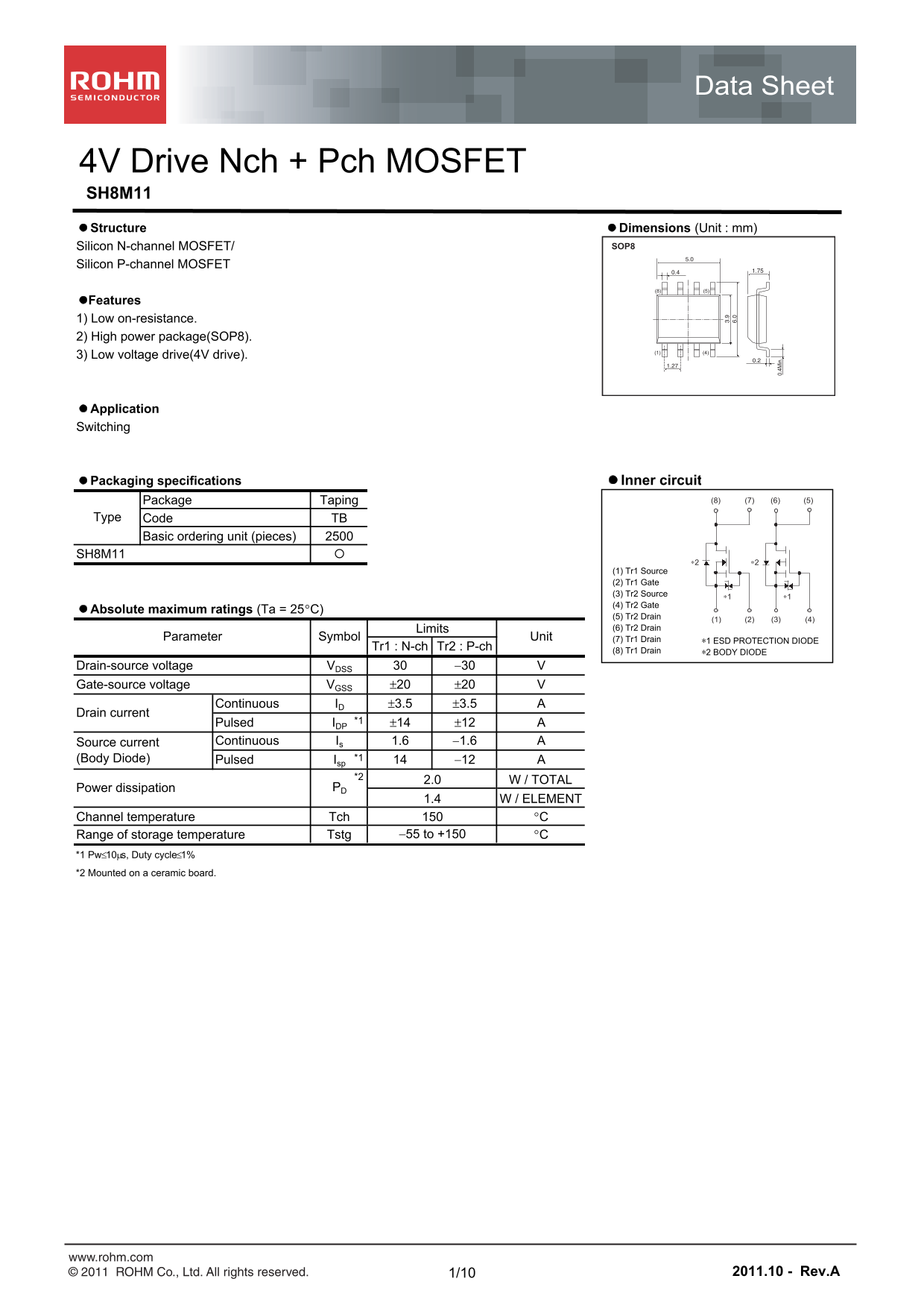
Page 1 Text Content
Data Sheet
4V Drive Nch + Pch MOSFET SH8M11 Structure Dimensions (Unit : mm)
Silicon N-channel MOSFET/ SOP8
Silicon P-channel MOSFET
Features 1) Low on-resistance. 2) High power package(SOP8).
3) Low voltage drive(4V drive).
Application Switching
Packaging specifications Inner circuit
Package Taping (8) (7) (6) (5)
Type Code TB Basic ordering unit (pieces) SH8M11
(1) Tr1 Source (2) Tr1 Gate (3) Tr2 Source ∗1 ∗1 (4) Tr2 Gate
Absolute maximum ratings (Ta = 25C)
(5) Tr2 Drain (1) (2) (3) (4) Limits (6) Tr2 Drain
Parameter Symbol Unit (7) Tr1 Drain
∗1 ESD PROTECTION DIODE
Tr1 : N-ch Tr2 : P-ch (8) Tr1 Drain
∗2 BODY DIODE
Drain-source voltage VDSS 30
Gate-source voltage VGSS 20 20
Continuous ID 3.5 3.5
Drain current
Pulsed IDP *1 14 12 Source current Continuous Is 1.6 1.6 (Body Diode) Pulsed Isp *1 12 *2
2.0 W / TOTAL
Power dissipation PD
1.4 W / ELEMENT
Channel temperature Tch C
Range of storage temperature Tstg 55 to +150 C
*1 Pw10s, Duty cycle1% *2 Mounted on a ceramic board.
www.rohm.com © 2011 ROHM Co., Ltd. All rights reserved. 1/10 2011.10 - Rev.A
Page Summary Contents For ROHM SH8M11 User Guide
Manual Details
| Brand | ROHM |
|---|---|
| Pages | 11 |
| File Size | 1.27 MB |
| Published | July 22, 2026 |
Enter the captcha to get the download link:

Frequently Asked Questions
Is ESD protection required when using this product?
Yes, users must consider designing an ESD protection circuit because the product might cause chip aging under large electrified environments.
What type of mounting surface is recommended?
The device must be mounted on a ceramic board for proper operation.
What are the maximum drain-source voltage ratings?
The absolute maximum ratings include VDS limits of -30V to +30V, and also specify body diode voltages.
What is the total allowed power dissipation (PD)?
The total allowable power dissipation (P d) is 2.0 W.
What are the general voltage drive requirements?
The manual specifies gate-source voltage (V gs) ratings of up to +/-20 V for operation.