ROHM RSU002P03 User Guide
Summary
This datasheet details the RSU002P03 Silicon P-channel MOSFET, an optimal switching component designed for applications requiring low on-resistance and 4V drive capabilities. This manual provides comprehensive electrical characteristics—including static readings, dynamic switching times, and body diode performance. It is essential technical documentation for electronics engineers, circuit designers, and technicians who require reliable and high-performance power transistors for robust electronic system development.
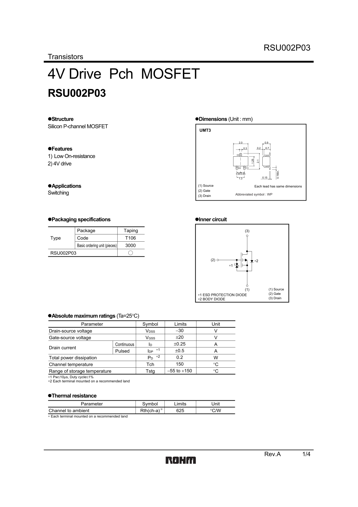
Page 1 Text Content
RSU002P03
Transistors
4V Drive Pch MOSFET RSU002P03 Structure Dimensions (Unit : mm) Silicon P-channel MOSFET
Features
1) Low On-resistance 2) 4V drive
Applications (1) Source Each lead has same dimensions (2) Gate
Switching Abbreviated symbol : WP
(3) Drain
Packaging specifications Inner circuit
Package Taping (3)
Type Code T106
Basic ordering unit (pieces)
RSU002P03 1. 2.
0. 1M in
(1) (1) Source (2) Gate
∗1 ESD PROTECTION DIODE
∗2 BODY DIODE (3) Drain
Absolute maximum ratings (Ta=25°C)
Parameter Symbol Limits Unit Drain-source voltage −30 VVDSS Gate-source voltage ±20 VVGSS Continuous ±0.25 AID
Drain current
Pulsed ±0.5 AIDP
Total power dissipation 0.2 WPD
Channel temperature °CTch
Range of storage temperature −55 to +150 °CTstg
∗1 Pw≤10µs, Duty cycle≤1% ∗2 Each terminal mounted on a recommended land
Thermal resistance
Parameter Symbol Limits Unit
Channel to ambient °C/WRth(ch-a)
∗ Each terminal mounted on a recommended land
Rev.A 1/4
Page Summary Contents For ROHM RSU002P03 User Guide
Manual Details
| Brand | ROHM |
|---|---|
| Pages | 5 |
| File Size | 63.18 KB |
| Published | July 15, 2026 |
Enter the captcha to get the download link:

Frequently Asked Questions
What is the maximum total power dissipation (PD)?
The maximum rated total power dissipation for this component is 0.2 W.
Can I use this transistor in life-critical applications like medical devices?
No; if your equipment requires extremely high reliability, you must consult a sales representative first.
What are the typical ranges for the drain current and resistance on-state performance?
Static on-state resistance (RDS(on)) typically ranges from 1.4 Ω to 2.4 Ω during operation.
Does proper circuit design affect thermal performance?
Yes, mounting each terminal on a recommended land is necessary for accurate thermal dissipation according to the manual.