ROHM RSD100N10 User Guide
Summary
This comprehensive datasheet introduces the RSD100N10 N-channel MOSFET, an ideal component engineered for high-power and efficiency demands. Featuring low on-resistance and optimized 4V drive capabilities, this device excels in demanding switching applications, ensuring reliable circuit performance. The manual provides power electronics engineers with exhaustive details, including absolute maximum ratings, detailed electrical curves (switching time, thermal resistance), and operational guidelines required for precise component selection and design validation.
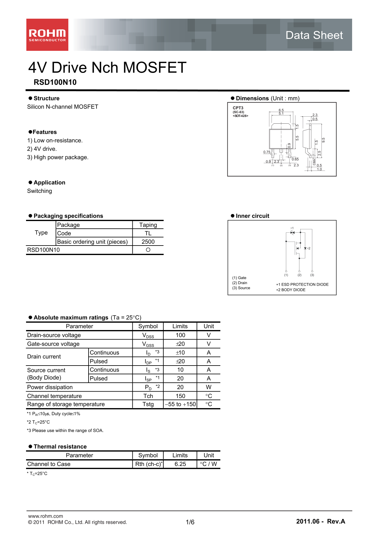
Page 1 Text Content
Data Sheet
4V Drive Nch MOSFET RSD100N10 Structure Dimensions (Unit : mm) Silicon N-channel MOSFET CPT3
(SC-63)
<SOT-428> 2.3 0.5
Features 1) Low on-resistance. 2) 4V drive.
3) High power package. 0.65
Application Switching
Packaging specifications Inner circuit
Package Taping
Type Code TL Basic ordering unit (pieces)
RSD100N10
(1) Gate (2) Drain
1 ESD PROTECTION DIODE
(3) Source 0.
2 BODY DIODE
0. 8M in.
Absolute maximum ratings (Ta = 25C) 2.
Parameter Symbol Limits Unit
Drain-source voltage VDSS Gate-source voltage VGSS 20
Continuous ID *3 10
Drain current
Pulsed IDP *1 20 Source current Continuous IS *3 (Body Diode) Pulsed ISP *1 Power dissipation PD *2
Channel temperature Tch C Range of storage temperature Tstg 55 to 150 C *1 PW10s, Duty cycle1% *2 TC=25°C *3 Please use within the range of SOA.
Thermal resistance
Parameter Symbol Limits Unit
Channel to Case Rth (ch-c) 6.25 C / W * TC=25°C
www.rohm.com
© 2011 ROHM Co., Ltd. All rights reserved. 1/6 2011.06 - Rev.A
Page Summary Contents For ROHM RSD100N10 User Guide
Manual Details
| Brand | ROHM |
|---|---|
| Pages | 7 |
| File Size | 1.13 MB |
| Published | June 22, 2026 |
Enter the captcha to get the download link:

Frequently Asked Questions
What is the maximum drain-source voltage (VDSS)?
The absolute maximum rating for VDS is 100V.
How much power can this MOSFET dissipate?
The maximum continuous power dissipation (PD) is rated at 20W.
Are there limits on operating the device?
Yes, operation must stay within the area shown in the Maximum Safe Operating Area (Fig.15).
What are the gate voltage parameters for operation?
The drain-source voltage Vd is rated up to 100V, and the gate-source voltage Vgs is $\pm20$V.