ROHM QST3 User Guide
Summary
A versatile general-purpose NPN transistor ideal for low-frequency amplification and driving applications. This comprehensive manual serves as an essential resource, detailing absolute maximum ratings, detailed electrical characteristics, saturation voltage curves, and performance metrics up to 200 MHz. It is designed for professional hardware engineers and electronics designers requiring high reliability in power amplifier and driver circuit development.
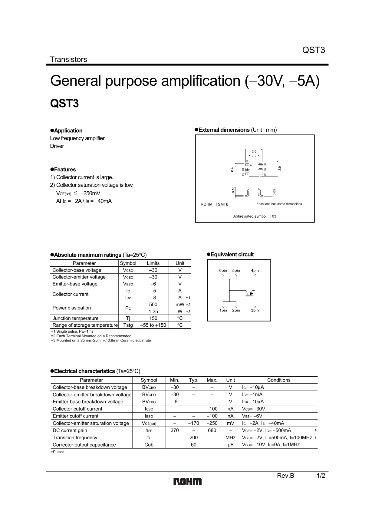
Page 1 Text Content
Transistors
General purpose amplification (−30V, −5A) QST3
Application External dimensions (Unit : mm)
Low frequency amplifier Driver
Features 1) Collector current is large. 2) Collector saturation voltage is low. VCE(sat) −250m V At IC = −2A / IB = −40m A
ROHM : TSMT6 Each lead has same dimensions
Abbreviated symbol : T03
Absolute maximum ratings (Ta=25°C) Equivalent circuit
Parameter Symbol Limits Unit (4 (5 (6
Collector-base voltage VCBO −30 6pin 5pin 4pin
Collector-emitter voltage VCEO −30
Emitter-base voltage VEBO −6 IC −5
Collector current
ICP −8 ∗1
Power dissipation PC
1pin 2pin 3pin
Junction temperature Tj °C Range of storage temperature Tstg −55 to +150 °C ∗1 Single pulse, Pw=1ms ∗2 Each Terminal Mounted on a Recommended ∗3 Mounted on a 25mm×25mm× 0.8mm Ceramic substratet
Electrical characteristics (Ta=25°C)
Parameter Symbol Min. Typ. Max. Unit Conditions
Collector-base breakdown voltage BVCBO −30 IC= −10µA Collector-emitter breakdown voltage BVCEO −30 IC= −1m A Emitter-base breakdown voltage BVEBO −6 IE= −10µA
Collector cutoff current ICBO −100 n A VCB= −30V
Emitter cutoff current IEBO −100 n A VEB= −6V Collector-emitter saturation voltage VCE(sat) −170 −250 m V IC= −2A, IB= −40m A DC current gain h FE VCE= −2V, IC= −500m A
Transition frequency f T MHz VCE= −2V, IE=500m A, f=100MHz Corrector output capacitance Cob p F VCB= −10V, IE=0A, f=1MHz
∗Pulsed
Rev.B 1/2
Page Summary Contents For ROHM QST3 User Guide
Manual Details
| Brand | ROHM |
|---|---|
| Pages | 3 |
| File Size | 62.77 KB |
| Published | July 12, 2026 |
Enter the captcha to get the download link:

Frequently Asked Questions
Should I use this transistor in equipment requiring extremely high reliability?
If used in life-critical applications, you must consult a sales representative before use.
What is the maximum power dissipation rating for the QST3?
The collector power dissipation (PC) limit is 500 mW when pulsed.
When mounting this device, what dimensions are specified for the ceramic substrate?
It must be mounted on a 25mm × 25mm × 0.8mm Ceramic substrate.
What is the typical DC current gain (hFE) reported for this transistor?
The highly rated collector-emitter current gain (hFE) ranges from 270 to 680.