ROHM QS8J11 User Guide
Summary
P-channel MOSFET designed for efficient switching applications, this component is engineered with low on-resistance and features a compact high-power package optimized for 1.5V drive systems. The accompanying technical manual and data sheet provide comprehensive electrical and thermal specifications essential for accurate circuit design. It covers absolute maximum ratings, static and dynamic characteristics (such as $R_{DS(on)}$ and switching times), thermal resistance, and detailed measurement procedures, making it ideal for power electronics engineers developing reliable, high-performance circuits.
Page 1 Text Content
Data Sheet
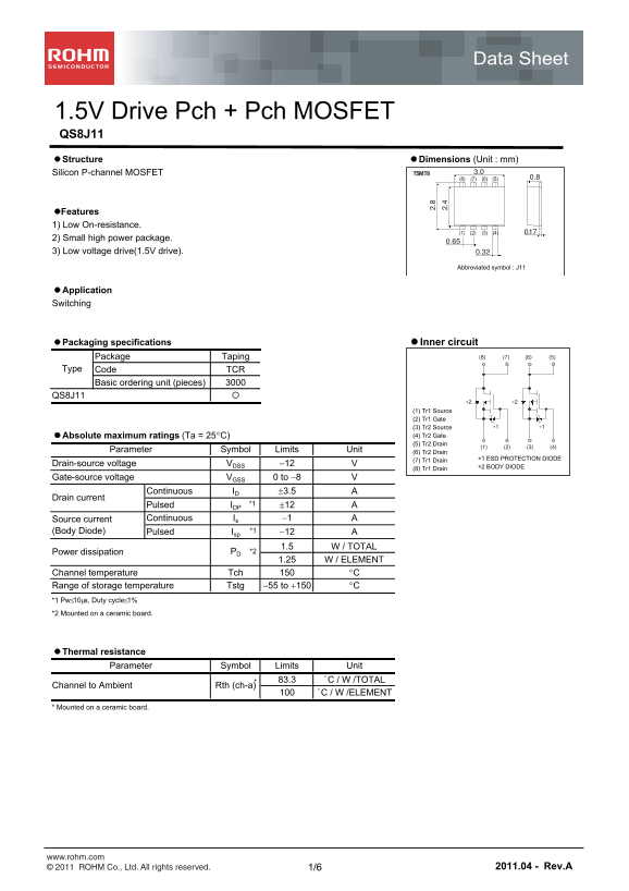
1.5V Drive Pch + Pch MOSFET QS8J11 Structure Dimensions (Unit : mm) Silicon P-channel MOSFET TSMT8
Features 1) Low On-resistance.
2) Small high power package. 3) Low voltage drive(1.5V drive).
Abbreviated symbol : J11
Application Switching
Packaging specifications Inner circuit
Package Taping (8) (7) (6) (5)
Type Code TCR Basic ordering unit (pieces) QS8J11
(1) Tr1 Source (2) Tr1 Gate
(3) Tr2 Source ∗1 ∗1
Absolute maximum ratings (Ta = 25C) (4) Tr2 Gate (5) Tr2 Drain
Parameter Symbol Limits Unit (6) Tr2 Drain
(7) Tr1 Drain ∗1 ESD PROTECTION DIODE
Drain-source voltage VDSS 12
(8) Tr1 Drain ∗2 BODY DIODE
Gate-source voltage VGSS 0 to 8 Continuous ID 3.5
Drain current
Pulsed IDP *1 12
Source current Continuous Is 1 (Body Diode) Pulsed Isp *1 12
1.5 W / TOTAL PDPower dissipation *2 1.25 W / ELEMENT
Channel temperature Tch C Range of storage temperature Tstg 55 to 150 C *1 Pw10s, Duty cycle1% *2 Mounted on a ceramic board.
Thermal resistance
Parameter Symbol Limits Unit
83.3 ˚C / W /TOTAL
Channel to Ambient Rth (ch-a)
˚C / W /ELEMENT
* Mounted on a ceramic board.
www.rohm.com © 2011 ROHM Co., Ltd. All rights reserved. 1/6 2011.04 - Rev.A
Page Summary Contents For ROHM QS8J11 User Guide
Manual Details
| Brand | ROHM |
|---|---|
| Pages | 7 |
| File Size | 1.22 MB |
| Published | June 05, 2026 |
Enter the captcha to get the download link:

Frequently Asked Questions
What is the maximum drain-source voltage (VDS) rating?
The absolute maximum rating for VDS is -12 V.
How much power dissipation is rated per element?
The maximum power dissipation (Pd) limit is 1.25 W / ELEMENT.
What is the typical static on-state resistance range?
Static Drain-Source On-State Resistance (Rds(on)) ranges from -55 to 82 mΩ, depending on operating conditions.
Are there specific instructions for handling electric environments?
Yes, the manual warns that this product might cause chip aging and breakdown under large electrified environments and advises designing an ESD protection circuit.