ROHM QS6U22 User Guide
Summary
This integrated semiconductor component is designed for load switching, DC/DC conversion, and essential ESD protection applications. It seamlessly combines a P-channel MOS FET with a Schottky Barrier Diode in a compact TSMT6 package, offering low on-state resistance and fast performance at a 2.5V drive voltage. The accompanying manual provides comprehensive technical data, including detailed electrical characteristics, absolute maximum ratings, and switching curves for engineers building reliable electronic circuits. This device is ideal for power management applications requiring high efficiency and robust protection.
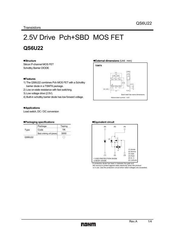
Page 1 Text Content
QS6U22
Transistors
2.5V Drive Pch+SBD MOS FET QS6U22
Structure External dimensions (Unit : mm) Silicon P-channel MOS FET
TSMT6
Schottky Barrier DIODE
1.0MAX
Features 1) The QS6U22 combines Pch MOS FET with a Schottky
barrier diode in a TSMT6 package. (1) (2) (3)
1pin mark
2) Low on-state resistance with fast switching. 0.16
3) Low voltage drive (2.5V).
Each lead has same dimensions
4) Built-in schottky barrier diode has low forward voltage. Abbreviated symbol : U22
Applications Load switch, DC / DC conversion
Packaging specifications Equivalent circuit 1. 2.
Package Taping (6) (5) (4)
Type Code TR
Basic ordering unit (pieces)
QS6U22
(1) Anode
(2) Source (3) Gate
(4) Drain (5) N / C
∗1 ESD PROTECTION DIODE
∗2 BODY DIODE (6) Cathode
∗A protection diode has been in between the gate and the source to protect against static electricity when the product is in use. Use the protection circuit when rated voltages are exceeded.
Rev.A 1/4
Page Summary Contents For ROHM QS6U22 User Guide
Manual Details
| Brand | ROHM |
|---|---|
| Pages | 5 |
| File Size | 83.54 KB |
| Published | June 04, 2026 |
Enter the captcha to get the download link:
