ROHM QS6M4 User Guide
Summary
The QS6M4 is a powerful, combined MOSFET integrated circuit housed in a TSMT6 package, ideal for robust power switching applications like load switches and inverters. This component features both P-channel and N-channel MOSFETs, delivering low on-state resistance and rapid switching capability with minimal 2.5V drive required. The accompanying manual provides comprehensive technical documentation, including detailed electrical characteristics, thermal limits, dynamic measurements, and absolute maximum ratings, helping engineers reliably design next-generation power electronics circuits.
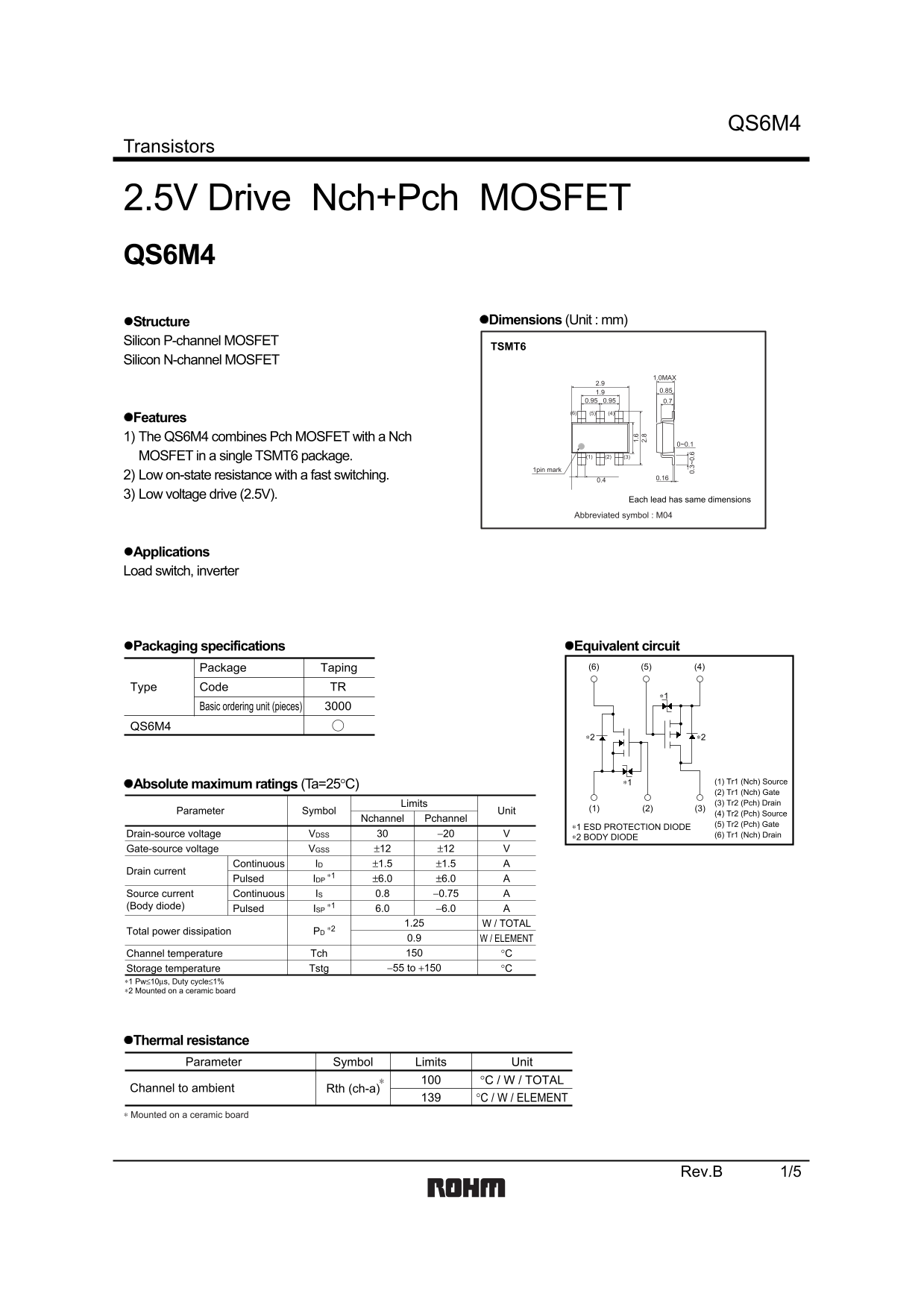
Page 1 Text Content
QS6M4
Transistors
2.5V Drive Nch+Pch MOSFET QS6M4
Structure Dimensions (Unit : mm)
Silicon P-channel MOSFET
TSMT6
Silicon N-channel MOSFET
1.0MAX
Features 1) The QS6M4 combines Pch MOSFET with a Nch
MOSFET in a single TSMT6 package. (1) (2) (3)
1pin mark
2) Low on-state resistance with a fast switching. 0.4 0.16
3) Low voltage drive (2.5V).
Each lead has same dimensions
Abbreviated symbol : M04
Applications Load switch, inverter
Packaging specifications Equivalent circuit Package Taping (6) (5) (4)
Type Code TR
Basic ordering unit (pieces)
QS6M4
∗1 (1) Tr1 (Nch) Source
Absolute maximum ratings (Ta=25°C)
(2) Tr1 (Nch) Gate Limits (3) Tr2 (Pch) Drain
Parameter Symbol Unit (1) (2) (3)
(4) Tr2 (Pch) Source
Nchannel Pchannel
∗1 ESD PROTECTION DIODE (5) Tr2 (Pch) Gate
Drain-source voltage VDSS −20 V30 ∗2 BODY DIODE (6) Tr1 (Nch) Drain Gate-source voltage VGSS ±12 V±12 Continuous ID ±1.5 A±1.5
Drain current
∗1 Pulsed IDP ±6.0 A±6.0 Continuous Source current IS −0.75 A0.8 (Body diode) ∗1 Pulsed ISP −6.0 A6.0
1.25 W / TOTAL
∗2 Total power dissipation PD
W / ELEMENT0.9 Channel temperature °CTch
Storage temperature −55 to +150 °CTstg
∗1 Pw≤10µs, Duty cycle≤1% ∗2 Mounted on a ceramic board
Thermal resistance Parameter Symbol Limits Unit
°C / W / TOTAL
Channel to ambient Rth (ch-a)
°C / W / ELEMENT
∗ Mounted on a ceramic board
Rev.B 1/5
Page Summary Contents For ROHM QS6M4 User Guide
Manual Details
| Brand | ROHM |
|---|---|
| Pages | 6 |
| File Size | 98.33 KB |
| Published | July 22, 2026 |
Enter the captcha to get the download link:

Frequently Asked Questions
What precautions should I take when designing into this product?
Always account for derating characteristics and implement sufficient safety features, such as anti-flammability or fail-safe measures.
What are the designated applications or usages for this MOSFET?
It is primarily designed to be used as a load switch or in an inverter circuit.
What does 'Tch' represent, and what is its limit?
'Tch' represents the Channel temperature, which must not exceed 150 °C.