ROHM QS5U17 User Guide
Summary
This comprehensive technical manual details the QS5U17, an integrated power component combining a low-voltage N-channel MOSFET with a Schottky Barrier Diode in one package. It is engineered for applications such as load switching and DC/DC conversion, offering fast switching and low on-state resistance at 2.5V drive. The guide provides essential deep dive specifications, including absolute maximum ratings, detailed electrical characteristics (e.g., switching times, capacitances), and usage graphs necessary for power electronics designers integrating reliable solid-state protection into their circuits.
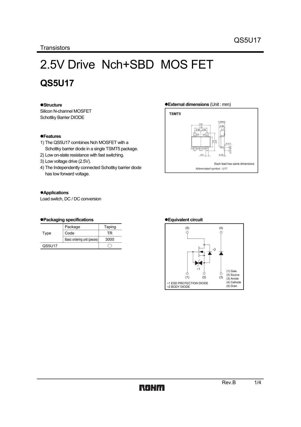
Page 1 Text Content
QS5U17
Transistors
2.5V Drive Nch+SBD MOS FET QS5U17
Structure External dimensions (Unit : mm)
Silicon N-channel MOSFET
TSMT5
Schottky Barrier DIODE
1.0MAX
Features 1) The QS5U17 combines Nch MOSFET with a 0~0.1
Schottky barrier diode in a single TSMT5 package. (1) (3)(2)
2) Low on-state resistance with fast switching. 0.4 0.16
3) Low voltage drive (2.5V).
Each lead has same dimensions
4) The Independently connected Schottky barrier diode Abbreviated symbol : U17 has low forward voltage.
Applications Load switch, DC / DC conversion
Packaging specifications Equivalent circuit
Package Taping (5) (4)
Type Code TR
Basic ordering unit (pieces)
QS5U17
(1) Gate (2) Source
(3) Anode (4) Cathode
∗1 ESD PROTECTION DIODE
∗2 BODY DIODE (5) Drain
Rev.B 1/4
Page Summary Contents For ROHM QS5U17 User Guide
Manual Details
| Brand | ROHM |
|---|---|
| Pages | 5 |
| File Size | 83.87 KB |
| Published | June 22, 2026 |
Enter the captcha to get the download link:

Frequently Asked Questions
What unique components does the QS5U17 package combine?
It combines an Nch MOSFET with a Schottky Barrier diode in a single TSMT5 package.
Is the QS5U17 suitable for life-critical applications like medical instruments?
No; users must consult a sales representative if the application requires extremely high reliability or endangers human life.
What is the minimum on-state resistance ($R_{DS(on)}$) for this MOSFET?
The static drain-source on-state resistance is rated from 76 to 10⁷ mΩ at specific operation points.
What is the recommended voltage range when using the device?
The drain-source voltage (DSS) limit is 30 V, and the gate-source voltage (VGSS) limit is 12 V.