ROHM BCX19 User Guide
Summary
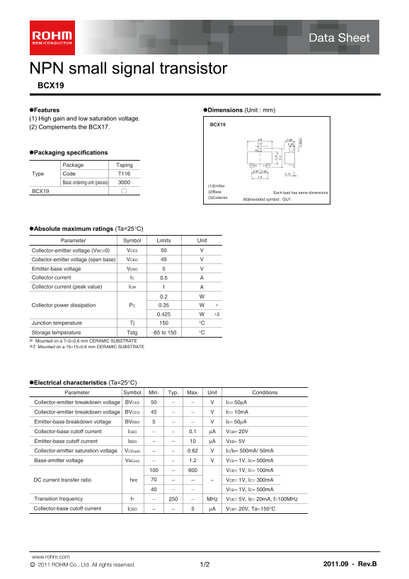
The BCX19 is a high-gain NPN small signal transistor designed for general electronic switching applications. This comprehensive manual provides detailed technical specifications, including absolute maximum ratings, electrical characteristics (like hFE and VCE(sat)), and performance graphs crucial for circuit design. It is essential reference material for electronics engineers and hardware designers building communication devices, appliances, or custom circuitry that requires reliable amplification and switching capability.
Page 1 Text Content
NPN small signal transistor BCX19 Features Dimensions (Unit : mm) (1) High gain and low saturation voltage.
BCX19
(2) Complements the BCX17.
Packaging specifications
Package Taping (2) (1) 0.95 0.95
Type Code T116 0.15
Basic ordering unit (pieces)
(1)Emitter
BCX19 (2)Base Each lead has same dimensions
(3)Collector
Abbreviated symbol : GU1
Absolute maximum ratings (Ta=25C)
Parameter Symbol Limits Unit
Collector-emitter voltage (VBE=0) VCES Collector-emitter voltage (open base) VCEO
Emitter-base voltage VEBO
Collector current 0.5IC
Collector current (peak value) ICM A1
0. 2M in
Collector power dissipation PC 0.35
Junction temperature Tj °C Storage temperature Tstg −65 to 150 °C
∗ Mounted on a 7×5×0.6 mm CERAMIC SUBSTRATE ∗2 Mounted on a 15×15×0.6 mm CERAMIC SUBSTRATE
Electrical characteristics (Ta=25C)
Parameter Symbol Min. Typ. Max. Unit Conditions
Collector-emitter breakdown voltage BVCES IC= 50μA
Collector-emitter breakdown voltage BVCEO IC= 10m A
Emitter-base breakdown voltage BVEBO IE= 50μA
Collector-base cutoff current ICBO 0.1 μA VCB= 20V
Emitter-base cutoff current IEBO μA VEB= 5V Collector-emitter saturation voltage VCE(sat) 0.62 IC/IB= 500m A/ 50m A
Base-emitter voltage VBE(on) 1.2 VCE= 1V, IC= 500m AV
VCE= 1V, IC= 100m A
DC current transfer ratio h FE VCE= 1V, IC= 300m A VCE= 1V, IC= 500m A
Transition frequency f T MHz VCE= 5V, IE= 20m A, f=100MHz
Collector-base cutoff current ICBO μA VCB= 20V, Ta=150°C
www.rohm.com
○c 2011 ROHM Co., Ltd. All rights reserved. 2011.09 1/2 Rev.B
Page Summary Contents For ROHM BCX19 User Guide
Manual Details
| Brand | ROHM |
|---|---|
| Pages | 3 |
| File Size | 199.78 KB |
| Published | June 21, 2026 |
Enter the captcha to get the download link:

Frequently Asked Questions
What are the absolute maximum ratings for this transistor?
The collector current ($I_C$) limit is 0.5 A, and the maximum collector power dissipation ($P_C$) is 0.35 W.
Can I use this component in systems requiring high reliability (e.g., medical or aerospace)?
No. The product is not designed for equipment where failure could result in a direct threat to human life or create a risk of human injury.
Do the example circuit diagrams guarantee successful operation in my specific design?
While they illustrate standard operations, peripheral conditions must be taken into account when designing circuits for mass production.
What is the maximum safe operating junction temperature for the BCX19?
The junction temperature ($T_j$) limit is specified up to 150 °C.