# A B C D E F G H I J K L M N O P Q R S T U V W X Y Z

RICOH RP550K001A 1A PWM VFM Dual Step-down DC DC Converter with Synchronous Rectifier Data Manual

Summary

The RP550K001A is a high-efficiency, 1A dual step-down DC/DC converter utilizing synchronous rectification for stable power conversion. Designed for portable electronics such as camcorders and notebooks, it offers adjustable output voltage (recommended range 0.6V to 3.3V) with minimal external components. The manual details its flexible operation modes, including automatic PWM/VFM switching for optimum efficiency. Key features include advanced protection circuits like UVLO and thermal shutdown, making it reliable and ideal for various battery-powered applications.
📄 Preview 📖 Table of Contents Contents PAGE OF 31

Page 1 Text Content

RP550K001A

1A* PWM/VFM Dual Step-down DC/DC Converter with Synchronous Rectifier

NO.EA-285-120328

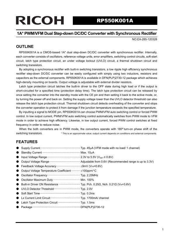
OUTLINE RP550K001A is a CMOS-based 1A* dual step-down DC/DC converter with synchronous rectifier. Internally, each converter consists of oscillators, reference voltage units, error amplifiers, switching control circuits, soft-start circuit, latch type protection circuit, an under voltage lockout (UVLO) circuit, a thermal shutdown circuit and switching transistors. By adopting a synchronous rectifier with built-in switching transistors, a low ripple high efficiency synchronous rectifier step-down DC/DC converter can be easily configured with simply using two inductors, resistors and capacitors as the external components. RP550K001A is available in DFN(PLP)2730-12 package which achieves high-density mounting on boards. Output voltage is adjustable with external divider resistors. Latch type protection circuit latches the built-in driver to the OFF state during high load or if the output is short-circuited for a specified time (protection delay time). The latch type protection circuit can be released by once setting the converter into the standby mode with the CE pin and then setting it back to the active mode, or, by turning the power off and back on. Setting the supply voltage lower than the UVLO detector threshold can also release the latch type protection circuit. Thermal shutdown circuit detects overheating of the converter and stops the converter operation to protect it from damage if the junction temperature exceeds the specified temperature. By inputting a signal to MODE pin, RP550K001A can choose PWM/VFM auto switching control or forced PWM control. In low output current, PWM/VFM auto switching control automatically switches from PWM mode to VFM mode in order to achieve high efficiency. Likewise, in low output current, forced PWM control switches at fixed frequency in order to reduce noise. When the both converters are in PWM mode, the converters operate with 180º turn-on phase shift of the switching transistors. * This is an approximate value; output current depends on conditions and external components.

FEATURES ● Supply Current ·················································· Typ. 45μA (VFM mode with no load/ 1 channel) ● Standby Current ················································ Max. 10μA ● Input Voltage Range·········································· 2.3V to 5.5V (VSET ≥ 0.8V) ● Output Voltage Range······································· Adjustable from 0.6V (Recommended range is up to 3.3V) ● Feedback Voltage Accuracy······························ ±9m V (VFB=0.6V) ● Output Voltage Temperature Coefficient ··········· ±100ppm/°C ● Oscillator Frequency ········································· Typ. 2.25MHz ● Oscillator Maximum Duty ·································· Min. 100% ● Built-in Driver ON Resistance ··························· Typ. Pch. 0.25Ω, Nch. 0.21Ω (VIN=3.6V) ● UVLO Detector Threshold································· Typ. 2.0V ● Soft Start Time··················································· Typ. 0.2ms ● Lx Current Limit Circuit······································ Typ. 1700m A/ channel ● Latch Type Protection Circuit ···························· Typ. 1.5ms ● Package ···························································· DFN(PLP)2730-12

Page Summary Contents For RICOH RP550K001A 1A PWM VFM Dual Step-down DC DC Converter with Synchronous Rectifier Data Manual

Page 1 RP550K001A 1A* PWM/VFM Dual Step-down DC/DC Converter with Synchronous Rectifier NO.EA-285-120328 OUTLINE RP550K001A is a CMOS-based 1A* dual step-down DC/DC converter with synchronous rectifier. Inte...
Page 2 RP550K001A APPLICATION Power source for portable communication equipment, camcorder, DSC, Notebook PC Power source for HDD, WLAN Power source for Li-ion battery-used equipment BLOCK DIAGRAM SLOPE CURR...
Page 3 RP550K001A SELECTION GUIDE Product Name Package Quantity per Reel Pb Free Halogen Free RP550K001A-TR DFN(PLP)2730-12 5,000pcs Yes Yes Output voltage is adjustable with external divider resistors. Reco...
Page 4 RP550K001A ABSOLUTE MAXIMUM RATINGS (AGND=PGND1=PGND2=0V) Symbol Item Rating Unit VIN VIN Input Pin Voltage -0.3 to 6.5 V VLX1, VLX2 LX1, LX2 Pin Voltage -0.3 to VIN + 0.3 V VCE1, VCE2 CE1, CE2 Pin Vo...
Page 5 RP550K001A ELECTRICAL CHARACTERISTICS Test Circuit is “OPEN LOOP” and Test Condition is AGND=PGND1=PGND2=0V, unless otherwise noted. RP550K001A (Ta=25°C) Symbol Item Conditions Min. Typ. Max. Unit 0.8...
Page 6 RP550K001A *1 For Standby Current, the sum of Channel 1 and Channel 2 is indicated. As for the following currents, either Channel 1 or Channel 2 is indicated. ・Supply Current 1 to Supply Current 3 ・CE...
Page 7 RP550K001A TYPICAL APPLICATION L1 2.2μH VOUT1 = 1.8V VIN 2.3V - 5.5V VIN LX1 COUT1 CE1 VFB1 MODE PGND1 RP550K001A L2 2.2μH VOUT2 = 2.5V VIN LX2 COUT2 CIN CE2 VFB2 AGND PGND2 Note: MODE= “H” Forced PWM...
Page 8 RP550K001A TECHNICAL NOTES When using RP550K001A, please consider the following points. AGND, PGND1 and PGND2 must be wired to the GND plane when mounting on boards. VIN pins must be wired to the VIN ...
Page 9 RP550K001A OPERATION OF STEP-DOWN DC/DC CONVERTER AND OUTPUT CURRENT The step-down DC/DC converter charges energy in the inductor when LX Tr. turns “ON”, and discharges the energy from the inductor wh...
Page 10 RP550K001A Discontinuous Mode and Continuous Mode As illustrated in Diag 3., when the output current (IOUTT) is relatively small, t OPEN < t OFF . In this case, the energy charged into the inductor...
Page 11 RP550K001A Forced PWM Mode and VFM Mode By setting the MODE pin to “H”, the IC switches the frequency at the fixed rate to reduce noise even when the output load is light. Therefore, when IOUT is ∆IL/...
Page 12 RP550K001A Output Current and Selection of External Components The following equations explain the relationship between output current and peripheral components used in the diagram in “TYPICAL APPLICA...
Page 13 RP550K001A TIMING CHART (1) Soft Start Time Starting-up with CE Pin The IC starts to operate when the CE pin voltage (VCE) exceed the threshold voltage. The threshold voltage is preset between CE “H” ...
Page 14 RP550K001A (2) Under Voltage Lockout (UVLO) Circuit If VIN becomes lower than the setting voltage (VSET), the step-down DC/DC converter stops the switching operation and ON duty becomes 100%, and then...
Page 15 RP550K001A (3) Over Current Protection Circuit, Latch Type Protection Circuit Over current protection circuit supervises the inductor peak current (the peak current flowing through Pch Tr.) in each sw...
Page 16 ut pu t V ol ta ge (V ut pu t V ol ta ge (V ut pu t V ol ta ge (V RP550K001A CHARACTERISTICS 1) Output Voltage vs. Output Current RP550K001A VOUT=0.6V RP550K001A VOUT=0.6V MODE=“L”PWM/VFM Auto Switchi...
Page 17 ut pu t V ol ta ge (V RP550K001A ut pu t V ol ta ge (V ut pu t V ol ta ge (V RP550K001A VOUT=1.8V RP550K001A VOUT=1.8V MODE=“L”PWM/VFM Auto Switching Control MODE=“H” Forced PWM Control Vin=3.6V Vin=3...
Page 18 Fe ed ac ol ta ge FB (V ut pu t V ol ta ge (V ffi ci en cy RP550K001A RP550K001A VOUT=1.8V RP550K001A VOUT=3.3V MODE=“H” Forced PWM Control MODE=“H” Forced PWM Control Iout=1m A Iout=100m A Iout=800m ...
Page 19 RP550K001A ffi ci en cy ffi ci en cy RP550K001A VOUT=1.2V RP550K001A VOUT=1.8V VIN=5.0V, VMODE=0V VIN=5.0V, VMODE=0V VIN=3.6V, VMODE=0V VIN=3.6V, VMODE=0V VIN=VMODE=5.0V VIN=VMODE=5.0V VIN=VMODE=3.6V ...
Page 20 Su pp ly ur re nt u A ut pu t R ip pl Vo lta ge (A RP550K001A rip pl (V 5) Supply Current vs. Ambient Temperature 6) Supply Current vs. Input Voltage RP550K001A VOUT=1.8V(VIN=5.5V) RP550K001A VOUT=1.8...
Page 21 RP550K001A ut pu t R ip pl ol ta ge (A ut pu t R ip pl ol ta ge (A Vr ip pl (V Vr ip pl (V RP550K001A VOUT=0.8V(VIN=3.6V) RP550K001A VOUT=0.8V(VIN=3.6V) MODE=“L”PWM/VFM Auto Switching Control MODE=“H”...
Page 22 ut pu t R ip pl ol ta ge (A ut pu t R ip pl ol ta ge (A RP550K001A Vr ip pl (V Vr ip pl (V RP550K001A VOUT=1.8V(VIN=3.6V) RP550K001A VOUT=1.8V(VIN=3.6V) MODE=“L”PWM/VFM Auto Switching Control MODE=“H”...
Page 23 of t S ta rt Ti ts ta rt RP550K001A (μ s) Fr eq ue nc fo sc (M z) LO ol ta ge VL (V 8) Oscillator Frequency vs. Ambient Temperature 9) Oscillator Frequency vs. Input Voltage 2.4 2.4 VIN=3.6V Temperatu...
Page 24 ch r. es is ta nc (Ω LX im it ur re nt LX LI (m In pu t V ol ta ge EH (V RP550K001A 12) CE Input Voltage vs. Ambient Temperature CE “H” Input Voltage (VIN=5.5V) CE “L” Input Voltage (VIN=2.3V) 1.10 1....
Page 25 RP550K001A ut pu t V ol ta ge (V ut pu t V ol ta ge (V ut pu t V ol ta ge (V 16) Load Transient Response RP550K001A (VIN=3.6V, VOUT=0.6V) RP550K001A (VIN=3.6V, VOUT=0.6V) MODE=“L”PWM/VFM Auto Switchin...
Page 26 ut pu t V ol ta ge (V ut pu t V ol ta ge (V ut pu t V ol ta ge (V RP550K001A RP550K001A (VIN=3.6V, VOUT=0.8V) RP550K001A (VIN=3.6V, VOUT=0.8V) MODE=“L”PWM/VFM Auto Switching Control MODE=“L”PWM/VFM Au...
Page 27 RP550K001A ut pu t V ol ta ge (V ut pu t V ol ta ge (V ut pu t V ol ta ge (V RP550K001A (VIN=3.6V, VOUT=1.2V) RP550K001A (VIN=3.6V, VOUT=1.2V) MODE=“L”PWM/VFM Auto Switching Control MODE=“L”PWM/VFM Au...
Page 28 ut pu t V ol ta ge (V ut pu t V ol ta ge (V ut pu t V ol ta ge (V RP550K001A RP550K001A (VIN=3.6V, VOUT=1.8V) RP550K001A (VIN=3.6V, VOUT=1.8V) MODE=“L”PWM/VFM Auto Switching Control MODE=“L”PWM/VFM Au...
Page 29 RP550K001A ut pu t V ol ta ge (V ut pu t V ol ta ge (V ut pu t V ol ta ge (V RP550K001A (VIN=5.0V, VOUT=3.3V) RP550K001A (VIN=5.0V, VOUT=3.3V) MODE=“L”PWM/VFM Auto Switching Control MODE=“L”PWM/VFM Au...
Page 30 ut pu t V ol ta ge (V ut pu t V ol ta ge (V RP550K001A 17) Mode Switching Waveform RP550K001A (VIN=3.6V, VOUT=1.2V, IOUT=1m A) RP550K001A (VIN=3.6V, VOUT=1.2V, IOUT=1m A) MODE=“L” --> MODE=“H” MODE...
Page 31 1. The products and the product specifications described in this document are subject to change or discontinuation of production without notice for reasons such as improvement. Therefore, before decid...