RICOH PWM Step-down DC DC Converter with switch function R5220x SERIES User's Manual
Summary
The R5220x Series is a high-efficiency CMOS DC/DC converter designed for versatile power management. This IC provides dual operation as both a highly efficient PWM step-down converter and an LDO, switchable via the MODE pin, ensuring low consumption current even at light loads. The accompanying manual details its core components, including soft-start, integrated protection circuits, and voltage regulation options. It is ideal for designers building portable electronics, such as communication equipment and specialized devices, requiring stable, customizable power solutions within a compact footprint.
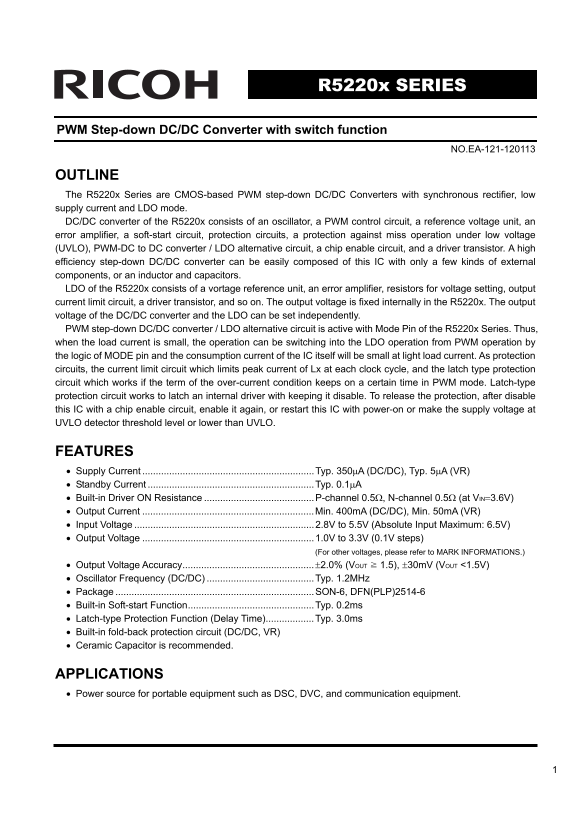
Page 1 Text Content
R5220x SERIES
PWM Step-down DC/DC Converter with switch function
NO.EA-121-120113
OUTLINE The R5220x Series are CMOS-based PWM step-down DC/DC Converters with synchronous rectifier, low supply current and LDO mode. DC/DC converter of the R5220x consists of an oscillator, a PWM control circuit, a reference voltage unit, an error amplifier, a soft-start circuit, protection circuits, a protection against miss operation under low voltage (UVLO), PWM-DC to DC converter / LDO alternative circuit, a chip enable circuit, and a driver transistor. A high efficiency step-down DC/DC converter can be easily composed of this IC with only a few kinds of external components, or an inductor and capacitors. LDO of the R5220x consists of a vortage reference unit, an error amplifier, resistors for voltage setting, output current limit circuit, a driver transistor, and so on. The output voltage is fixed internally in the R5220x. The output voltage of the DC/DC converter and the LDO can be set independently. PWM step-down DC/DC converter / LDO alternative circuit is active with Mode Pin of the R5220x Series. Thus, when the load current is small, the operation can be switching into the LDO operation from PWM operation by the logic of MODE pin and the consumption current of the IC itself will be small at light load current. As protection circuits, the current limit circuit which limits peak current of Lx at each clock cycle, and the latch type protection circuit which works if the term of the over-current condition keeps on a certain time in PWM mode. Latch-type protection circuit works to latch an internal driver with keeping it disable. To release the protection, after disable this IC with a chip enable circuit, enable it again, or restart this IC with power-on or make the supply voltage at UVLO detector threshold level or lower than UVLO.
FEATURES • Supply Current ................................................................Typ. 350μA (DC/DC), Typ. 5μA (VR) • Standby Current ..............................................................Typ. 0.1μA • Built-in Driver ON Resistance .........................................P-channel 0.5Ω, N-channel 0.5Ω (at VIN=3.6V) • Output Current ................................................................Min. 400m A (DC/DC), Min. 50m A (VR) • Input Voltage ...................................................................2.8V to 5.5V (Absolute Input Maximum: 6.5V) • Output Voltage ................................................................1.0V to 3.3V (0.1V steps)
(For other voltages, please refer to MARK INFORMATIONS.)
• Output Voltage Accuracy.................................................±2.0% (VOUT 1.5), ±30m V (VOUT <1.5V) • Oscillator Frequency (DC/DC) ........................................Typ. 1.2MHz • Package ..........................................................................SON-6, DFN(PLP)2514-6 • Built-in Soft-start Function...............................................Typ. 0.2ms • Latch-type Protection Function (Delay Time)..................Typ. 3.0ms • Built-in fold-back protection circuit (DC/DC, VR) • Ceramic Capacitor is recommended.
APPLICATIONS • Power source for portable equipment such as DSC, DVC, and communication equipment.
Page Summary Contents For RICOH PWM Step-down DC DC Converter with switch function R5220x SERIES User's Manual
Manual Details
| Brand | Ricoh |
|---|---|
| Pages | 21 |
| File Size | 408.16 KB |
| Published | June 05, 2026 |
Enter the captcha to get the download link:

Frequently Asked Questions
What is the primary difference between DC/DC mode and LDO mode?
The R5220x features a PWM-DC to LDO alternative circuit controlled by the MODE pin. In LDO mode, it operates efficiently at low load currents.
How do I reset the latch-type protection circuit after an over-current event?
To release the protection, use either the chip enable circuit (disable then re-enable), or restart the IC with power-on, or bring the supply voltage to the UVLO threshold level or lower.
What are the required input and output voltage ranges for operation?
The Input Voltage range is 2.8V to 5.5V (with an absolute maximum of 6.5V). The Output Voltage can be set between 1.0V and 3.3V in 0.1V steps.
What supplies the R5220x with low current consumption when lightly loaded?
The IC consumes a low operational current through switching into LDO mode via the MODE pin, ensuring small power draw at light load currents.