RICOH R5325x SERIES 150mA Dual LDO REGULATOR Data Sheet User Manual
Summary
This dual LDO voltage regulator IC is ideal for designing reliable power supplies in low-power, battery-operated equipment like hand-held communication devices and cameras. Featuring ultra-low supply standby current (Typ. 0.1μA), excellent transient response, and high stability, these CMOS regulators ensure prolonged battery life while maintaining precise output voltage regulation. The comprehensive manual details technical specifications, pinouts, selection guides, and application parameters, assisting engineers in integrating this powerful thermal management solution into dense board designs using SOT-23-6 or DFN(PLP)1820-6 packages.
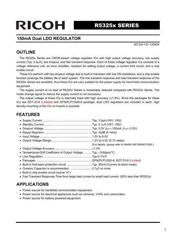
Page 1 Text Content
R5325x SERIES
150m A Dual LDO REGULATOR
NO.EA-127-120404
OUTLINE The R5325x Series are CMOS-based voltage regulator ICs with high output voltage accuracy, low supply current (Typ. 3.0μA), low dropout, and fast transient response. Each of these voltage regulator ICs consists of a voltage reference unit, an error amplifier, resistors for setting output voltage, a current limit circuit, and a chip enable circuit. These ICs perform with low dropout voltage due to built-in transistor with low ON resistance, and a chip enable function prolongs the battery life of each system. The line transient response and load transient response of the R5325x Series are excellent, thus these ICs are very suitable for the power supply for hand-held communication equipment. The supply current at no load of R5325x Series is remarkably reduced compared with R5323x Series. The mode change signal to reduce the supply current is not necessary. The output voltage of these ICs is internally fixed with high accuracy (±1.0%). Since the packages for these ICs are SOT-23-6 (Limited) and DFN(PLP)1820-6 package, dual LDO regulators are included in each, high density mounting of the ICs on boards is possible.
FEATURES • Supply Current ..............................................................Typ. 3.0µA (VR1, VR2) • Standby Current ............................................................Typ. 0.1μA (VR1, VR2) • Dropout Voltage ............................................................Typ. 0.2V (IOUT=150m A ,VOUT=3.0V) • Ripple Rejection............................................................Typ. 55d B (f=1k Hz) • Input Voltage .................................................................1.5V to 6.0V • Output Voltage Range...................................................1.2V to 4.0V (0.1V steps) (For details, please refer to MARK INFORMATIONS.) • Output Voltage Accuracy...............................................±1.0% • Temperature-Drift Coefficient of Output Voltage ...........Typ. ±100ppm/°C • Line Regulation .............................................................Typ.0.1%/V • Packages .....................................................................DFN(PLP)1820-6, SOT-23-6 (Limited) • Built-in fold-back protection circuit ................................Typ. 50m A (Current at short mode) • Ceramic Capacitor is recommended. ..........................0.1μF or more • Built-in chip enable circuit (active “H”) • Fast Transient Response Time from large load current to small load current. (50% less than R5323x)
APPLICATIONS • Power source for handheld communication equipment. • Power source for electrical appliances such as cameras, VCRs and camcorders. • Power source for battery-powered equipment.
Page Summary Contents For RICOH R5325x SERIES 150mA Dual LDO REGULATOR Data Sheet User Manual
Manual Details
| Brand | Ricoh |
|---|---|
| Pages | 20 |
| File Size | 528.07 KB |
| Published | June 04, 2026 |
Enter the captcha to get the download link:

Frequently Asked Questions
What is the recommended capacitor type when implementing this IC?
It is recommended to use a ceramic capacitor with a value of 0.1μF or greater.
How low are the standby current draw for both regulators (VR1, VR2)?
The typical standby current consumption is very low at 0.1μA.
Does it feature built-in protection against short circuits?
Yes, it includes a built-in fold-back protection circuit rated up to approximately 50mA during a short mode.
What type of devices are best suited for powering with this regulator?
It is suitable as a power source for handheld communication equipment and various battery-powered appliances.