# A B C D E F G H I J K L M N O P Q R S T U V W X Y Z

RICOH R5323x Series 150mA Dual LDO REGULATOR Data Sheet

Summary

The R5323x is a high-accuracy, dual LDO voltage regulator IC optimized for low power consumption and reliable performance in portable systems. This manual serves as a comprehensive guide for engineers, detailing electrical specifications, pin configurations, available packages (WLCSP, DFN, SOT-23), and selection parameters across various output voltages (1.5V–4.0V). It is specifically designed for power management in battery-powered equipment, such as handheld communication devices and cameras, requiring robust transient response and minimal standby current.
📄 Preview PAGE OF 24

Page 1 Text Content

R5323x SERIES

150m A Dual LDO REGULATOR

NO.EA-089-120404

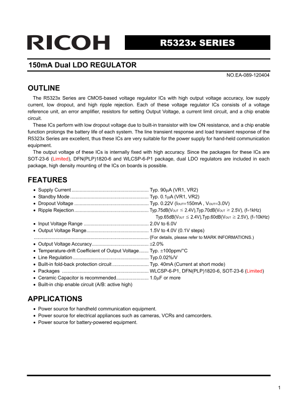
OUTLINE The R5323x Series are CMOS-based voltage regulator ICs with high output voltage accuracy, low supply current, low dropout, and high ripple rejection. Each of these voltage regulator ICs consists of a voltage reference unit, an error amplifier, resistors for setting Output Voltage, a current limit circuit, and a chip enable circuit. These ICs perform with low dropout voltage due to built-in transistor with low ON resistance, and a chip enable function prolongs the battery life of each system. The line transient response and load transient response of the R5323x Series are excellent, thus these ICs are very suitable for the power supply for hand-held communication equipment. The output voltage of these ICs is internally fixed with high accuracy. Since the packages for these ICs are SOT-23-6 (Limited), DFN(PLP)1820-6 and WLCSP-6-P1 package, dual LDO regulators are included in each package, high density mounting of the ICs on boards is possible.

FEATURES • Supply Current Typ. 90μA (VR1, VR2) • Standby Mode Typ. 0.1μA (VR1, VR2) • Dropout Voltage Typ. 0.22V (IOUT=150m A , VOUT=3.0V) • Ripple Rejection....................................................... Typ.75d B(VOUT 2.4V),Typ.70d B(VOUT 2.5V), (f=1k Hz)

Typ.65d B(VOUT 2.4V),Typ.60d B(VOUT 2.5V), (f=10k Hz)

• Input Voltage Range 2.0V to 6.0V • Output Voltage Range.............................................. 1.5V to 4.0V (0.1V steps)

(For details, please refer to MARK INFORMATIONS.)

• Output Voltage Accuracy.......................................... ±2.0% • Temperature-drift Coefficient of Output Voltage....... Typ. ±100ppm/°C • Line Regulation Typ.0.02%/V • Built-in fold-back protection circuit Typ. 40m A (Current at short mode) • Packages ................................................................ WLCSP-6-P1, DFN(PLP)1820-6, SOT-23-6 (Limited) • Ceramic Capacitor is recommended........................ 1.0μF or more • Built-in chip enable circuit (A/B: active high)

APPLICATIONS • Power source for handheld communication equipment. • Power source for electrical appliances such as cameras, VCRs and camcorders. • Power source for battery-powered equipment.

Page Summary Contents For RICOH R5323x Series 150mA Dual LDO REGULATOR Data Sheet

Page 1 R5323x SERIES 150m A Dual LDO REGULATOR NO.EA-089-120404 OUTLINE The R5323x Series are CMOS-based voltage regulator ICs with high output voltage accuracy, low supply current, low dropout, and high rip...
Page 2 BLOCK DIAGRAMS R5323xxxx A CE1 VOUT1 Error Amp. R1_1 Current Limit VDD GND Error Amp. Current Limit CE2 VOUT2 R5323xxxx B CE1 VOUT1 Error Amp. R1_1 Current Limit VDD GND Error Amp. Current Limit CE2 V...
Page 3 SELECTION GUIDE The output voltage, auto discharge function, package, etc. for the ICs can be selected at the user’s request. Product Name Package Quantity per Reel Pb Free Halogen Free R5323Zxxx∗-TR-...
Page 4 PIN CONFIGURATION • WLCSP-6-P1 • DFN(PLP)1820-6 • SOT-23-6 Mark Side Bump Side Top View Bottom View (mark side) PIN DESCRIPTIONS • WLCSP-6-P1 Pin No Symbol Pin Description 1 VOUT1 Output Pin 1 2 VDD I...
Page 5 • SOT-23-6 (Limited) Pin No Symbol Pin Description 1 VOUT1 Output Pin 1 2 VDD Input Pin 3 VOUT2 Output Pin 2 4 CE2 Chip Enable Pin 2 ("H" Active) 5 GND Ground Pin 6 CE1 Chip Enable Pin 1 (&q...
Page 6 ELECTRICAL CHARACTERISTICS • R5323xxxx A/B Topt=25°C Symbol Item Conditions Min. Typ. Max. Unit VOUT Output voltage VIN−VOUT=1.0V 1m A IOUT 30m A ×0.98 ×1.02 IOUT Output Current VIN−VOUT=1.0V 150 m A ...
Page 7 TYPICAL APPLIATION CE2 VOUT2 OUT2 Series IN VDD GND CE1 VOUT1 OUT1 C1=C2=C3=Ceramic 1.0μF TECHNICAL NOTES When using these ICs, consider the following points: Phase Compensation In these ICs, phase co...
Page 8 TEST CIRCUIT CE2 VOUT2 CE2 VOUT2 VOUT2 IOUT2 C3 Series Series VDD GND VDD GND CE1 VOUT1 CE1 VOUT1 IOUT1 C1 C1 VOUT1 C2 C1=C2=C3=Ceramic 1.0μF C1=C2=C3=Ceramic 1.0μF Fig.1 Standard test Circuit Fig.2 S...
Page 9 ut pu t V ol ta ge (V ut pu t V ol ta ge (V ut pu t V ol ta ge (V TYPICAL CHARACTERISTICS 1) Output Voltage vs. Output Current (Topt=25°C) 1.5V (VR1) 1.5V (VR2) VIN=3.5V VIN=3.5V 1.4 1.4 1.2 VIN=1.8V ...
Page 10 R5323x ut pu t V ol ta ge (V ut pu t V ol ta ge (V ut pu t V ol ta ge (V 2) Output Voltage vs. Input Voltage (Topt=25°C) 1.5V (VR1) 1.5V (VR2) Input Voltage VIN(V) Input Voltage VIN(V) 2.8V (VR1) 2.8V...
Page 11 ro po ut ol ta ge IF (V ro po ut ol ta ge IF (V ro po ut ol ta ge IF (V 3) Dropout Voltage vs. Output Current 1.5V (VR1) 1.5V (VR2) Topt= 85°C Topt= 85°C 0.5 25°C 0.5 25°C -40°C -40°C Output Current I...
Page 12 ut pu t V ol ta ge (V ut pu t V ol ta ge (V ut pu t V ol ta ge (V 4) Output Voltage vs. Temperature 1.5V (VR1) 1.5V (VR2) VIN=2.5V, IOUT=30m A VIN=2.5V, IOUT=30m A Temperature Topt(°C) Temperature Top...
Page 13 up pl ur re nt IS (μ up pl ur re nt IS (μ up pl ur re nt IS (μ 5) Supply Current vs. Input Voltage (Topt=25°C) 1.5V 2.8V VR1 VR1 VR2 VR2 Input Voltage VIN(V) Input Voltage VIN(V) up pl ur re nt IS (μ ...
Page 14 R5323x up pl ur re nt IS (μ up pl ur re nt IS (μ ro po ut ol ta ge IF (V 2.8V (VR1) 2.8V (VR2) VIN=3.8V VIN=3.8V Temperature Topt(°C) Temperature Topt(°C) 4.0V (VR1) 4.0V (VR2) VIN=5.0V VIN=5.0V up pl...
Page 15 ip pl ej ec tio (d ip pl ej ec tio (d ip pl ej ec tio (d 8) Ripple Rejection vs. Frequency (Topt=25°C) 1.5V (VR1) 1.5V (VR2) VIN=2.5V+0.5Vp-p, COUT=Ceramic 1.0μF VIN=2.5V+0.5Vp-p, COUT=Ceramic 1.0μF I...
Page 16 R5323x ip pl ej ec tio (d ip pl ej ec tio (d ip pl ej ec tio (d 2.8V (VR1) 2.8V (VR2) VIN=3.8V+0.5Vp-p, COUT=Ceramic 2.2μF VIN=3.8V+0.5Vp-p, COUT=Ceramic 2.2μF IOUT=1m A IOUT=1m A IOUT=30m A IOUT=30m ...
Page 17 ip pl ej ec tio (d ip pl ej ec tio (d ip pl ej ec tio (d 9) Ripple Rejection vs. Input Voltage (DC bias) (COUT=Ceramic 1.0μF, Topt=25°C) 2.8V (VR1) 2.8V (VR2) IOUT=1m A IOUT=1m A f=1k Hz f=1k Hz f=10k...
Page 18 ut pu t V ol ta ge (V ut pu t V ol ta ge (V ut pu t V ol ta ge (V 10) Input Transient Response (IOUT=30m A, tr=tf=5μs) R5323N001x(2.8V, VR1) IOUT=30m A, tr=tf=5μs, COUT=Ceramic 1.0μF Time T(μs) R5323N...
Page 19 R5323N001x(2.8V, VR2) ut pu t V ol ta ge (V ut pu t V ol ta ge (V ut pu t V ol ta ge (V Topt=25°C, COUT=Ceramic 1.0μF Time T(μs) R5323N001x(2.8V, VR2) Topt=25°C, COUT=Ceramic 2.2μF In pu t V ol ta ge ...
Page 20 ut pu t V ol ta ge (V ut pu t V ol ta ge (V ut pu t V ol ta ge (V 11) Load Transient Response 2.8V (VR1) 2.8V (VR1) CIN=Ceramic 1.0μF, COUT=Ceramic 1.0μF CIN=Ceramic 1.0µF, COUT=Ceramic 2.2µF 3.00 IOU...
Page 21 12) Minimum Operating Voltage 1.5V Minimum Operating Voltage Range VIN(MIN) Output Current IOUT(m A)
Page 22 ESR vs. Output Current When using these ICs, consider the following points: The relations between IOUT (Output Current) and ESR of an output capacitor are shown below. The conditions when the white no...
Page 23 R5323Z 1.5V (VR1/VR2) R5323Z 2.8V (VR1/VR2) VIN=2.5V VIN=3.8V CIN=COUT=Ceramic 1.0μF CIN=COUT=Ceramic 1.0μF Output Current IOUT(m A) Output Current IOUT(m A)
Page 24 1. The products and the product specifications described in this document are subject to change or discontinuation of production without notice for reasons such as improvement. Therefore, before decid...

Manual Details

Brand Ricoh
Pages 24
File Size 345.71 KB
Published June 01, 2026
89 views

Enter the captcha to get the download link:

captcha

Frequently Asked Questions

What capacitor type and value are recommended for operation?

A ceramic capacitor of 1.0μF or more is recommended.

What is the typical current draw during standby mode?

The typical standby current (VR1, VR2) is 0.1μA.

How can I determine the specific output voltage for each channel?

The output voltage can be set in the range from 1.5V to 4.0V in 0.1V steps, determined by serial numbers.

Does this regulator feature overcurrent protection?

Yes, it includes a built-in fold-back protection circuit with a typical current of 40mA (Current at short mode).