RICOH R1141Q SERIES User's Manual (1) Owner's Manual
Summary
This ultra-stable CMOS voltage regulator from the R1141Q series is engineered for reliable power management in space-constrained, battery-powered electronics. Featuring high output accuracy, low dropout voltage, and built-in protection features, it ensures reliable performance with minimal power consumption. The comprehensive manual provides system designers with critical electrical characteristics, application guides, specifications, and selection criteria. It is the ideal solution for powering handheld communication equipment, portable cameras, or any battery-dependent device requiring a highly stable, low-noise voltage source.
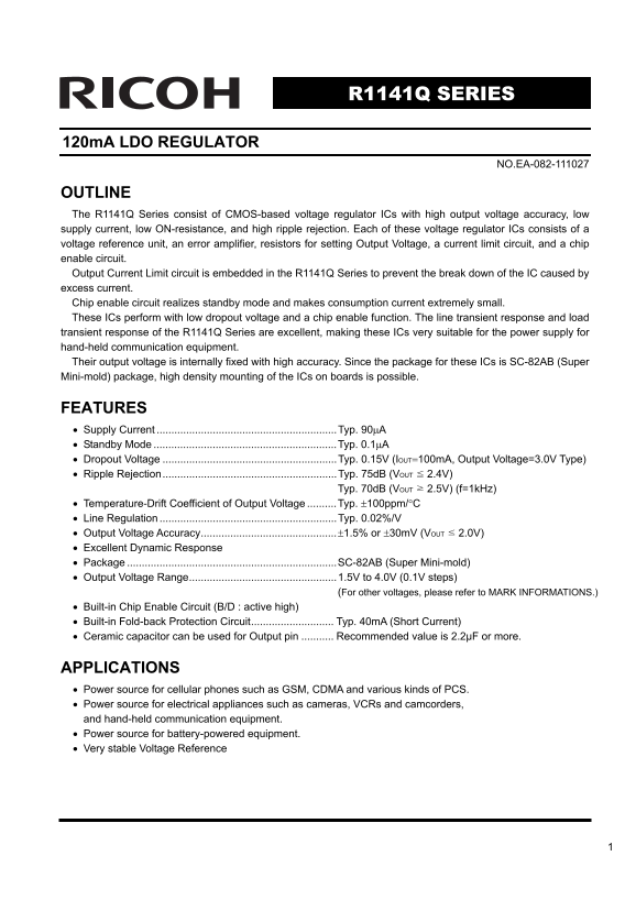
Page 1 Text Content
R1141Q SERIES
120m A LDO REGULATOR
NO.EA-082-111027
OUTLINE The R1141Q Series consist of CMOS-based voltage regulator ICs with high output voltage accuracy, low supply current, low ON-resistance, and high ripple rejection. Each of these voltage regulator ICs consists of a voltage reference unit, an error amplifier, resistors for setting Output Voltage, a current limit circuit, and a chip enable circuit. Output Current Limit circuit is embedded in the R1141Q Series to prevent the break down of the IC caused by excess current. Chip enable circuit realizes standby mode and makes consumption current extremely small. These ICs perform with low dropout voltage and a chip enable function. The line transient response and load transient response of the R1141Q Series are excellent, making these ICs very suitable for the power supply for hand-held communication equipment. Their output voltage is internally fixed with high accuracy. Since the package for these ICs is SC-82AB (Super Mini-mold) package, high density mounting of the ICs on boards is possible.
FEATURES • Supply Current .............................................................Typ. 90μA • Standby Mode ..............................................................Typ. 0.1μA • Dropout Voltage ...........................................................Typ. 0.15V (IOUT=100m A, Output Voltage=3.0V Type) • Ripple Rejection...........................................................Typ. 75d B (VOUT 2.4V)
Typ. 70d B (VOUT 2.5V) (f=1k Hz)
• Temperature-Drift Coefficient of Output Voltage ..........Typ. ±100ppm/°C • Line Regulation ............................................................Typ. 0.02%/V • Output Voltage Accuracy..............................................±1.5% or ±30m V (VOUT 2.0V) • Excellent Dynamic Response • Package .......................................................................SC-82AB (Super Mini-mold) • Output Voltage Range..................................................1.5V to 4.0V (0.1V steps) (For other voltages, please refer to MARK INFORMATIONS.) • Built-in Chip Enable Circuit (B/D : active high) • Built-in Fold-back Protection Circuit............................ Typ. 40m A (Short Current) • Ceramic capacitor can be used for Output pin Recommended value is 2.2µF or more.
APPLICATIONS • Power source for cellular phones such as GSM, CDMA and various kinds of PCS. • Power source for electrical appliances such as cameras, VCRs and camcorders, and hand-held communication equipment. • Power source for battery-powered equipment. • Very stable Voltage Reference
Page Summary Contents For RICOH R1141Q SERIES User's Manual (1) Owner's Manual
Manual Details
| Brand | Ricoh |
|---|---|
| Pages | 16 |
| File Size | 253.48 KB |
| Published | May 29, 2026 |
Enter the captcha to get the download link:

Frequently Asked Questions
What type and value of capacitor should I use on the output pin?
A ceramic capacitor is recommended, with a minimum value of 2.2µF or more.
How does this circuit manage power consumption during standby mode?
The built-in Chip Enable Circuit allows for standby mode, resulting in an extremely small typical supply current of 0.1μA.
What is the maximum operational input voltage (VIN)?
The absolute maximum rating for the Input Voltage (VIN) is 6.5 V.
Does the regulator protect against short circuits or excessive output current?
Yes, it features a built-in Fold-back Protection Circuit that typically activates around 40mA during a short current condition.