# A B C D E F G H I J K L M N O P Q R S T U V W X Y Z

RICOH RP503x SERIES Data Sheet (1) User Manual

Summary

The RP503x Series offers a highly efficient 600mA step-down DC/DC converter utilizing a synchronous rectifier optimized for portable electronics. This low-ripple chip features automatic PWM/VFM switching, ensuring maximum efficiency even at low output currents while maintaining robust protection circuits. The manual provides comprehensive details on operation specifications, voltage selection (0.8V to 2.5V), and package options. Ideal for engineers designing battery-powered medical equipment, cameras, or general handheld communication devices requiring reliable and stable power sources.
📄 Preview PAGE OF 29

Page 1 Text Content

RP503x SERIES

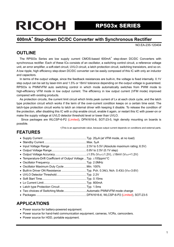
600m A∗ Step-down DC/DC Converter with Synchronous Rectifier

NO.EA-235-120404

OUTLINE The RP503x Series are low supply current CMOS-based 600m A∗ step-down DC/DC Converters with synchronous rectifier. Each of these ICs consists of an oscillator, a switching control circuit, a reference voltage unit, an error amplifier, a soft-start circuit, UVLO circuit, a latch protection circuit, switching transistors, and so on. A low ripple, high efficiency step-down DC/DC converter can be easily composed of this IC with only an inductor and capacitors. In terms of the output voltage, since the feedback resistances are built-in, the voltage is fixed internally. 0.1V step output can be set by laser-trim and 1.5% or 18m V tolerance depending on the output voltage is guaranteed. RP503x is PWM/VFM auto switching control in which mode automatically switches from PWM mode to high-efficiency VFM mode in low output current. The efficiency in low output current (VFM mode) improved compared with existing products. As protection circuits, the current limit circuit which limits peak current of Lx at each clock cycle, and the latch type protection circuit which works if the term of the over-current condition keeps on a certain time exist. The latch-type protection circuit works to latch an internal driver with keeping it disable. To release the condition of the protection, after disabling this IC with a chip enable circuit, enable it again, or restart this IC with power-on or make the supply voltage at UVLO detector threshold level or lower than UVLO. Since packages are WLCSP-6-P2 (Limited), DFN1616-6, SOT-23-5, high density mounting on boards is possible.

∗)This is an approximate value, because output current depends on conditions and external parts.

FEATURES • Supply Current ......................................................Typ. 20μA (at VFM mode, at no load) • Standby Current ....................................................Max. 5μA • Input Voltage Range .............................................2.5V to 5.5V (Absolute maximum rating; 6.5V) • Output Voltage Range...........................................0.8V to 2.5V (0.1V step) • Output Voltage Accuracy.......................................±1.5% (VOUT≥1.2V), ±18m V (VOUT<1.2V) • Temperature-Drift Coefficient of Output Voltage ...Typ. ±100ppm/°C • Oscillator Frequency .............................................Typ. 2.0MHz • Oscillator Maximum Duty Cycle............................Min. 100% • Built-in Driver ON Resistance ...............................Typ. Pch. 0.34Ω, Nch. 0.43Ω (VIN=3.6V) • UVLO Detector Threshold.....................................Typ. 2.2V • Soft Start Time.......................................................Typ. 0.15ms • Lx Current Limit.....................................................Typ. 800m A • Latch type Protection Circuit .................................Typ. 1.5ms • Two choices of Switching Mode............................Automatic PWM/VFM mode change • Packages ..............................................................DFN1616-6, WLCSP-6-P2 (Limited), SOT-23-5

APPLICATIONS • Power source for battery-powered equipment. • Power source for hand-held communication equipment, cameras, VCRs, camcorders. • Power source for HDD, portable equipment.

Page Summary Contents For RICOH RP503x SERIES Data Sheet (1) User Manual

Page 1 RP503x SERIES 600m A∗ Step-down DC/DC Converter with Synchronous Rectifier NO.EA-235-120404 OUTLINE The RP503x Series are low supply current CMOS-based 600m A∗ step-down DC/DC Converters with synchron...
Page 2 RP503x BLOCK DIAGRAMS RP503Zxx1A (Limited) RP503Lxx1A Chip Ramp Current Enable Compensation Feedback OSC Current Protection PWM Switching Control Control Soft Start VOUT RP503Zxx2A (Limited) RP503Lxx2...
Page 3 RP503x RP503Nxx1A Chip Ramp Current Enable Compensation Feedback OSC Current Protection PWM Switching Control Control Soft Start VOUT RP503Nxx2A Chip Ramp Current Enable Compensation Feedback OSC Curr...
Page 4 RP503x SELECTION GUIDE The output voltage, auto discharge function, and package for the ICs can be selected at the user’s request. Product Name Package Quantity per Reel Pb Free Halogen Free RP503Zxx∗...
Page 5 RP503x PIN CONFIGURATIONS • WLCSP-6-P2 • DFN1616-6 • SOT-23-5 Mark Side Bump Side Top View Bottom View (mark side) PIN DESCRIPTIONS • WLCSP-6-P2 (Limited) Pin No Symbol Pin Description 1 VOUT Output P...
Page 6 RP503x ABSOLUTE MAXIMUM RATINGS AGND=PGND=0V Symbol Item Rating Unit VIN Input Voltage −0.3 to 6.5 V VLx Lx pin Voltage −0.3 to VIN+0.3 V VCE CE Pin Input Voltage −0.3 to 6.5 V VOUT Output Voltage −0....
Page 7 RP503x ELECTRICAL CHARACTERISTICS • RP503x Topt=25°C Symbol Item Conditions Min. Typ. Max. Unit VIN Operating Input Voltage 2.5 5.5 V VOUT ≥ 1.2V ×0.985 ×1.015 VOUT Output Voltage VIN=VCE=3.6V VOUT &l...
Page 8 RP503x TEST CIRCUITS CE VOUT CE VOUT RP503x RP503x Series Series PGNDAGND PGNDAGND VIN LX VIN LX OSCILLOSCOPE OSCILLOSCOPE Output Voltage Oscillator Frequency CE VOUT CE VOUT RP503x RP503x Series Seri...
Page 9 RP503x CE VOUT CE VOUT RP503x RP503x Series Series PGNDAGND PGNDAGND OSCILLOSCOPE VIN LX VIN LX Lx Leakage Current CE Input Voltage CE VOUT CE VOUT RP503x RP503x Series Series PGNDAGND PGNDAGND OSCILL...
Page 10 RP503x TYPICAL APPLICATION VIN VOUT VIN LX 4.7μHRP503L/Z Series CIN COUT CE VOUT PGNDAGND RP503L/Zxxx A VIN VOUT VIN LX RP503N CIN Series COUT CE VOUT RP503Nxxx A Symbol Parts Recommendation CIN 4.7μF...
Page 11 RP503x TECHNICAL NOTES When using these ICs, consider the following points: ⋅ Set the same level as AGND and PGND. ⋅ Set external components such as an inductor, CIN, COUT as close as possible to the ...
Page 12 RP503x Operation of step-down DC/DC converter and Output Current The DC/DC converter charges energy in the inductor when LX transistor is ON, and discharges the energy from the inductor when LX transi...
Page 13 RP503x Discontinuous mode and Continuous mode When the output current (IOUT) is relatively small, topen &lt; toff as illustrated in the above diagram. In this case, the energy is charged in the induct...
Page 14 RP503x Output Current and selection of External components The relation between the output current and external components is as follows: (Wherein, Ripple Current p-p value is described as IRP, ON res...
Page 15 RP503x TIMING CHART (1) Soft Start Time • In the case of starting this IC with CE In the case of starting this IC with CE, the operation can be as in the timing chart below. When the voltage of CE pin...
Page 16 RP503x (2) Under Voltage Lockout (UVLO) Circuit The step-down DC/DC converter stops and ON duty becomes 100%, if input voltage (VIN) becomes less than the set output voltage (Set VOUT), the output vol...
Page 17 RP503x (3) Over Current Protection Circuit, Latch Type Protection Circuit Over current protection circuit supervises the coil peak current (the current flowing Pch transistor) at each switching cycle,...
Page 18 ut pu t V ol ta ge (V ut pu t V ol ta ge (V ut pu t V ol ta ge (V RP503x TYPICAL CHARACTERISTICS* 1) Output Voltage vs. Output Current RP503x08x A (VFM MODE) RP503x08x A (PWM MODE) VIN=3.6V VIN=3.6V 0...
Page 19 ut pu t V ol ta ge (V ut pu t V ol ta ge (V ut pu t V ol ta ge (V RP503x RP503x25x A (VFM MODE) RP503x25x A (PWM MODE) 2.54 2.54 2.53 VIN=3.6V VIN=3.6V 2.52 VIN=5.0V VIN=5.0V Output Current IOUT (m A)...
Page 20 ut pu t V ol ta ge (V ffi ci en cy ffi ci en cy RP503x 3) Output Voltage vs. Temperature RP503x15x A VOUT=1.5V ffi ci en cy -50 -25 ffi ci en cy Temperature Topt (°C) 4) Efficiency vs. Output Current ...
Page 21 ut pu t R ip pl Vo lta ge AC Vr ip pl (V ffi ci en cy up pl ur re nt (µ RP503x RP503x25x A VIN=3.6V VIN=5.0V Output Current IOUT (m A) In du ct or ur re nt IL (m A) ut pu t R ip pl Vo lta ge AC 5) Sup...
Page 22 ut pu t R ip pl Vo lta ge AC ut pu t R ip pl Vo lta ge AC ut pu t R ip pl Vo lta ge AC Vr ip pl (V Vr ip pl (V Vr ip pl (V RP503x RP503x12x A RP503x12x A IOUT=10m A IOUT=250m A 0.04 Output Voltage 0.0...
Page 23 Fr eq ue nc fo sc (M z) LO ol ta ge VL 1 ( So ft ta rt Ti ta rt (µ s) RP503x 8) Oscillator Frequency vs. Temperature 9) Oscillator Frequency vs. Input Voltage RP503x15x A RP503x15x A 2.40 2.20 VIN=3.6...
Page 24 In pu t V ol ta ge (V Lx ur re nt im it Ili (m ch r. es is ta nc (Ω RP503x 12) CE Input Voltage vs. Temperature CE&quot;H&quot; Input Voltage CE&quot;L&quot; Input Voltage RP503x15x A RP503x15x A 1.0 ...
Page 25 ut pu t V ol ta ge (V RP503x ut pu t V ol ta ge (V ut pu t V ol ta ge (V 16) Turn on speed with CE pin (VIN=3.6V, Topt=25°C) RP503x08x A RP503x08x A ROUT=1kΩ ROUT=130Ω CE Input Voltage CE Input Voltag...
Page 26 ut pu t V ol ta ge (V ut pu t V ol ta ge (V ut pu t V ol ta ge (V RP503x RP503x25x A RP503x25x A ROUT=1kΩ ROUT=130Ω CE Input Voltage CE Input Voltage Output Voltage Output Voltage ut pu t C ur re nt (...
Page 27 ut pu t V ol ta ge (V ut pu t V ol ta ge (V ut pu t V ol ta ge (V RP503x RP503x12x A RP503x12x A Output Current 300m A--&gt;1m A Output Voltage 1.15 1.15 Output Voltage ut pu t C ur re nt (m A) ut pu ...
Page 28 ut pu t V ol ta ge (V ut pu t V ol ta ge (V ut pu t V ol ta ge (V RP503x RP503x18x A RP503x18x A Output Current 500m A--&gt;200m A Output Current 200m A--&gt;500m A Output Voltage 1.75 Output Voltage ...
Page 29 1. The products and the product specifications described in this document are subject to change or discontinuation of production without notice for reasons such as improvement. Therefore, before decid...

Manual Details

Brand Ricoh
Pages 29
File Size 881.15 KB
Published June 01, 2026
67 views

Enter the captcha to get the download link:

captcha

Frequently Asked Questions

What is the output voltage accuracy range?

The accuracy is ±1.5% when VOUT≥1.2V, and ±18mV when VOUT<1.2V.

How does this converter operate efficiently at low loads?

It uses PWM/VFM auto switching control, which automatically switches to high-efficiency VFM mode at low output current.

What are the built-in protection features?

It includes a current limit circuit (limiting peak Lx current) and a latch type protection circuit activated by over-current conditions for a certain time.

What is the required input voltage range?

The ideal input voltage range is 2.5V to 5.5V, with an absolute maximum rating of 6.5V.