# A B C D E F G H I J K L M N O P Q R S T U V W X Y Z

RICOH RP501K SERIES Data Manual (1) User Guide

Summary

The RP501K series provides a sophisticated solution for step-down DC/DC conversion using integrated CMOS technology and synchronous rectifiers. This efficient converter generates low ripple, stable power (1.0V–3.3V) with built-in protection features like UVLO and current limiting. The associated manual details the IC's architecture, operational modes, package specifications, and application guidelines. It is ideal for designers creating portable electronics, including cellular devices, PCs, battery-powered equipment, and vehicle accessories.
📄 Preview PAGE OF 32

Page 1 Text Content

RP501K SERIES

1A Step-down DC/DC Converters with synchronous rectifier

NO.EA-199-111124

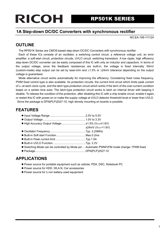
OUTLINE The RP501K Series are CMOS-based step-down DC/DC Converters with synchronous rectifier. Each of these ICs consists of an oscillator, a switching control circuit, a reference voltage unit, an error amplifier, a soft-start circuit, protection circuits, UVLO circuit, switching transistors. A low ripple, high efficiency step-down DC/DC converter can be easily composed of this IC with only an inductor and capacitors. In terms of the output voltage, since the feedback resistances are built-in, the voltage is fixed internally. 50m V (custom-made) step output can be set by laser-trim and ±1.5% or ±24m V tolerance depending on the output voltage is guaranteed. Mode alternative circuit works automatically for improving the efficiency. Considering fixed noise frequency, PWM fixed control type is also available. As protection circuits, the current limit circuit which limits peak current of LX at each clock cycle, and the latch type protection circuit which works if the term of the over-current condition keeps on a certain time exist. The latch-type protection circuit works to latch an internal driver with keeping it disable. To release the condition of the protection, after disabling this IC with a chip enable circuit, enable it again, or restart this IC with power-on or make the supply voltage at UVLO detector threshold level or lower than UVLO. Since the package is DFN(PLP)2527-10, high density mounting on boards is possible.

FEATURES Input Voltage Range ..............................................2.5V to 5.5V Output Voltage .......................................................1.0V to 3.3V High Accuracy Output Voltage ...............................±1.5% (VOUT≥1.6V) ±24m V (VOUT<1.6V) Oscillator Frequency..............................................Typ. 2.25MHz Built-in Soft start Function......................................Max.0.2ms Built-in Peak current limit .......................................Typ.1.5A Built-in UVLO Function ..........................................Typ. 2.2V Switching Mode can be controlled by Mode pin ....Automatic PWM/VFM mode change / PWM fixed Package .................................................................DFN(PLP)2527-10

APPLICATIONS Power source for portable equipment such as cellular, PDA, DSC, Notebook PC Power source for HDD, WLA N, Car accessories Power source for Li-ion battery-used equipment

Page Summary Contents For RICOH RP501K SERIES Data Manual (1) User Guide

Page 1 RP501K SERIES 1A Step-down DC/DC Converters with synchronous rectifier NO.EA-199-111124 OUTLINE The RP501K Series are CMOS-based step-down DC/DC Converters with synchronous rectifier. Each of these IC...
Page 2 RP501K BLOCK DIAGRAM RP501Kxx1A CHIP SLOPE CURRENT ENABLE COMPENSATION FEEDBACK OSCILLATOR CURRENT PROTECTION LX SWITCHING PWM/VFM CONTROL CONTROL SOFT VOUT UVLO START MODE AGND PGND TEST1 TEST2 RP501...
Page 3 RP501K Selection Guide In the RP501K series, output voltage and version can be designated with user's request. Part number can be designated as follows: Product Name Package Quantity per Reel Pb Free ...
Page 4 RP501K PIN CONFIGURATION DFN(PLP)2527-10 TOP VIEW BOTTOM VIEW PIN DESCRIPTIONS Pin No. Symbol Pin Description 1 CE Chip Enable Pin (“H” Active) 2 TEST1 Test Pin 1 (Connect this pin to the GND) 3 AGND ...
Page 5 RP501K ABSOLUTE MAXIMUM RATINGS (AGND=PGND=0V) Symbol Item Rating Unit AVIN AVIN Supply Voltage -0.3 to 6.5 V PVIN PVIN Supply Voltage -0.3 to 6.5 V VLX LX Pin Voltage -0.3 to A/PVIN+0.3 V VCE CE Pin ...
Page 6 RP501K ELECTRICAL CHARACTERISTICS RP501Kxx1x Ta=25°C Symbol Item Condition Min. Typ. Max. Unit A/PVIN Operating Input Voltage 2.5 5.5 V A/PVIN=VCE=3.6V, VMODE=0V VOUT Step-down Output Voltage VOUT≥1.6...
Page 7 RP501K TEST CIRCUITS CE VOUT CE VOUT AVINTEST1 AVINTEST1 RP501K RP501K Series Series AGND MODE AGND MODE PGND TEST2 PGND TEST2 LX PVIN LX PVIN OSCILLOSCOPE OSCILLOSCOPE Output Voltage Oscillator Frequ...
Page 8 RP501K CE VOUT CE VOUT AVINTEST1 AVINTEST1 RP501K RP501K Series Series AGND MODE AGND MODE PGND TEST2 PGND TEST2 LX PVIN LX PVIN OSCILLOSCOPE OSCILLOSCOPE Soft-start Time UVLO Detector Voltage / Relea...
Page 9 RP501K TYPICAL APPLICATION CE VOUT TEST1 AVIN RP501 SERIES PGND TEST2 CIN COUT Parts Recommendation CIN: 10µF Ceramic (C1608JB0J106K , TDK) COUT: 4.7µF Ceramic (C1608JB1A475K , TDK) L: 2.2µH (NR3010T2...
Page 10 RP501K Operation of step-down DC/DC converter and Output Current The DC/DC converter charges energy in the inductor when LX transistor is ON, and discharges the energy from the inductor when LX transi...
Page 11 RP501K Discontinuous mode and Continuous mode When the output current (IOUT) is relatively small, topen &lt; toff as illustrated in the following diagram. In this case, the energy is charged in the in...
Page 12 RP501K Output Current and selection of External components The relation between the output current and external components is as follows: When P-channel Tr. of LX is ON: (Wherein, Ripple Current P-P v...
Page 13 RP501K TIMING CHART (1) Soft Start Time In the case of starting this IC with CE In the case of starting this IC with CE, the operation can be as in the timing chart below. When the voltage of CE pin (...
Page 14 RP501K (2) Under Voltage Lockout (UVLO) Circuit The step-down DC/DC converter stops and ON duty becomes 100%, if input voltage (VIN) becomes less than the set output voltage (Set VOUT), the output vol...
Page 15 RP501K (3) Over Current Protection Circuit, Latch Type Protection Circuit Over current protection circuit supervises the coil peak current (the current flowing Pch transistor) at each switching cycle,...
Page 16 RP501K ffi ci en cy ffi ci en cy ffi ci en cy TYPICAL CHARACTERISTICS 1) Efficiency vs. Output Current 1-1 Input Voltage Dependence RP501K121x(PWM fixed) RP501K121x(PWM/VFM mode change) MODE=0V MODE=V...
Page 17 RP501K ffi ci en cy ffi ci en cy ffi ci en cy RP501K331x(PWM fixed) RP501K331x(PWM/VFM mode change) MODE=0V MODE=VIN Output CUrrent(m A) Output Current(m A) 1-2 Temperature Dependence Ef fic ie nc y( ...
Page 18 RP501K ut pu t V ol ta ge (V ffi ci en cy ffi ci en cy RP501K181x(PWM fixed) RP501K181x(PWM/VFM mode change) VIN=3.6V,MODE=0V VIN=MODE=3.6V Output Current(m A) Output Current(m A) ut pu t V ol ta ge (...
Page 19 RP501K ut pu t V ol ta ge (V ut pu t V ol ta ge (V ut pu t V ol ta ge (V RP501K151x(PWM fixed) RP501K151x(PWM/VFM mode change) MODE=0V MODE=VIN Output Current(m A) Output Current(m A) ut pu t V ol ta ...
Page 20 RP501K ut pu t V ol ta ge (V ut pu t V ol ta ge (V ut pu t V ol ta ge (V 2-2 Temperature Dependence RP501K121x(PWM fixed) RP501K121x(PWM/VFM mode change) VIN=3.6V,MODE=0V VIN=MODE=3.6V Output Current(...
Page 21 RP501K ut pu t V ol ta ge (V ut pu t V ol ta ge (V ut pu t V ol ta ge (V RP501K331x(PWM fixed) RP501K331x(PWM/VFM mode change) VIN=5.0V,MODE=0V VIN=MODE=5.0V Output Current Output Current(m A) ut pu t...
Page 22 RP501K ut pu t V ol ta ge (V ut pu t V ol ta ge (V ut pu t V ol ta ge (V RP501K181x(PWM fixed) RP501K181x(PWM/VFM modechange) MODE=0V MODE=VIN ,IOUT=1m A Input Voltage(V) Input Voltage(V) ut pu t V ol...
Page 23 RP501K ut pu t V ol ta ge (V ut pu t V ol ta ge (V ut pu t V ol ta ge (V RP501K151x(PWM fixed) RP501K151x(PWM/VFM mode change) VIN=3.6V,MODE=0V,IOUT=500m A VIN=MODE=3.6V ,IOUT=1m A Temperature(℃) Temp...
Page 24 RP501K ut pu t V ol ta ge (V ut pu t V ol ta ge (V ut pu t V ol ta ge (V 5) DC/DC Output Waveform (CIN=10μF, COUT=4.7μF, L=2.2μH) RP501K121x(PWM fixed) RP501K121x(PWM/VFM mode change) VIN=3.6V,MODE=0V...
Page 25 RP501K Fr eq ue nc y( z) up pl ur re nt (μ ut pu t V ol ta ge (V RP501K331x(PWM fixed) RP501K331x(PWM/VFM mode change) VIN=5.0V,MODE=0V,ROUT=10ohm VIN=MODE=5.0V ,ROUT=1kohm Time(μs) Time(μs) 6) Supply...
Page 26 RP501K of t-s ta rt Ti e( μs I/O ol ta ge (V I/O ol ta ge (V 10) Soft-start Time vs. Temperature RP501Kxx1x VIN=3.6V Temperature(℃) 11) Turn on waveform with CE pin (CIN=10μF, COUT= 4.7μF, L=2.2μH) I/...
Page 27 RP501K In pu t V ol ta ge (V I/O ol ta ge (V I/O ol ta ge (V 12) Turn off waveform with CE pin (CIN=10μF, COUT=4.7μF, L=2.2μH) RP501K121B RP501K151B VIN=3.6V,ROUT=1kohm VIN=3.6V,ROUT=1kohm CE CE OUT O...
Page 28 RP501K Tr . O es is ta nc e( oh Lx im it ur re nt (A Th re sh ol ol ta ge (V 14) CE Input vs. Temperature 15) MODE Input vs. Temperature RP501Kxx1x RP501Kxx1x Input Voltage Dependence Input Voltage De...
Page 29 RP501K ut pu t V ol ta ge (V ut pu t V ol ta ge (V ut pu t V ol ta ge (V 20) Load Transient Response (CIN=10μF, COUT=4.7μF, L=2.2μH) RP501K121x RP501K121x VIN=3.6V,MODE=0V,IOUT=0.5A to 0.8A VIN=3.6V,M...
Page 30 RP501K ut pu t V ol ta ge (V ut pu t V ol ta ge (V ut pu t V ol ta ge (V RP501K151x RP501K151x VIN=MODE=3.6V,IOUT=0.001A to 0.25A VIN=MODE=3.6V,IOUT=0.25A to 0.001A 1.40 OUT 0.75 1.45 0.75 1.35 0.50 1...
Page 31 RP501K ut pu t V ol ta ge (V ut pu t V ol ta ge (V RP501K331x RP501K331x VIN=5.0V,MODE=0V,IOUT=0.5A to 0.8A VIN=5.0V,MODE=0V,IOUT=0.8A to 0.5A 3.20 OUT 1.1 3.25 1.1 3.15 0.8 3.20 OUT 0.8 ut pu t C ur ...
Page 32 1. The products and the product specifications described in this document are subject to change or discontinuation of production without notice for reasons such as improvement. Therefore, before decid...

Manual Details

Brand Ricoh
Pages 32
File Size 1.17 MB
Published May 29, 2026
86 views

Enter the captcha to get the download link:

captcha

Frequently Asked Questions

What is the input voltage range for this converter?

The acceptable PVIN and AVIN supply voltage range is -0.3V to 6.5V.

How can I automate or fix the switching control mode?

You can select the mode using the MODE pin: Mode="H" defaults to PWM/VFM alternative, while setting it to "L" uses fixed PWM control.

What is the mechanism for releasing the over-current latch protection?

To reset the latch type protection circuit, you must either disable and re-enable the IC via the chip enable circuit, or perform a power-on/restart.

Does this converter handle low current draws or high-power devices?

The device is suitable for portable equipment (like cell phones) and has a built-in peak current limit of Typ. 1.5A.