# A B C D E F G H I J K L M N O P Q R S T U V W X Y Z

RICOH R1232D SERIES Data Handbook (1) Owner's Manual

Summary

The R1232D Series is a highly efficient, CMOS-based PWM step-down DC/DC converter featuring an integrated synchronous rectifier. Designed for engineers building reliable power sources, this IC delivers low ripple and high accuracy in converting voltage used in portable electronics like PDAs, notebooks, and HDDs. The accompanying manual provides comprehensive technical specifications, including configurable output voltages (adjustable or fixed), multiple oscillator frequencies, various protection circuits (UVLO, current limit), and detailed guidelines for implementing the converter with minimal external components.
📄 Preview PAGE OF 23

Page 1 Text Content

R1232D SERIES

PWM STEP-DOWN DC/DC CONVERTER WITH SYNCHRONOUS RECTIFIER

NO.EA-129-111123

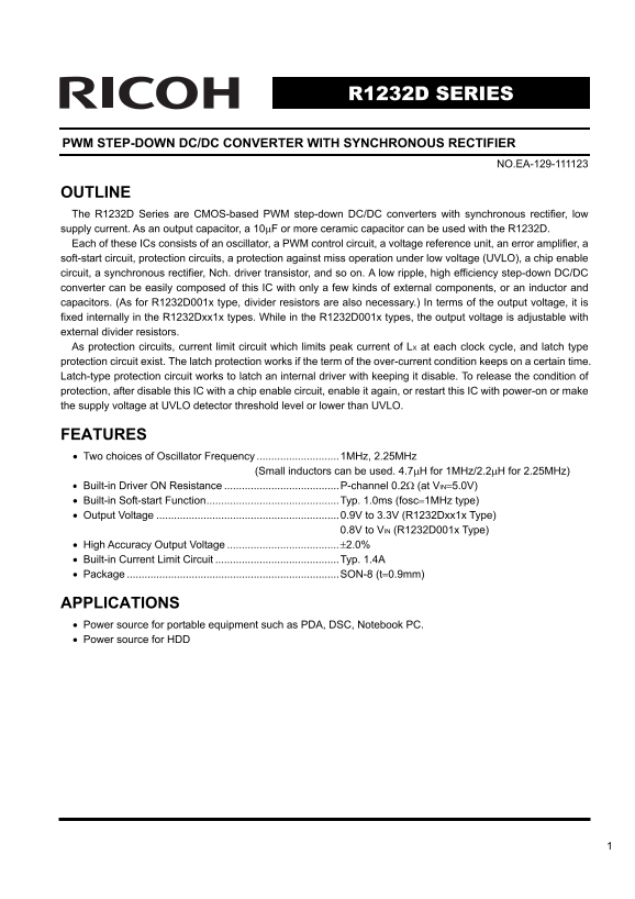
OUTLINE The R1232D Series are CMOS-based PWM step-down DC/DC converters with synchronous rectifier, low supply current. As an output capacitor, a 10μF or more ceramic capacitor can be used with the R1232D. Each of these ICs consists of an oscillator, a PWM control circuit, a voltage reference unit, an error amplifier, a soft-start circuit, protection circuits, a protection against miss operation under low voltage (UVLO), a chip enable circuit, a synchronous rectifier, Nch. driver transistor, and so on. A low ripple, high efficiency step-down DC/DC converter can be easily composed of this IC with only a few kinds of external components, or an inductor and capacitors. (As for R1232D001x type, divider resistors are also necessary.) In terms of the output voltage, it is fixed internally in the R1232Dxx1x types. While in the R1232D001x types, the output voltage is adjustable with external divider resistors. As protection circuits, current limit circuit which limits peak current of LX at each clock cycle, and latch type protection circuit exist. The latch protection works if the term of the over-current condition keeps on a certain time. Latch-type protection circuit works to latch an internal driver with keeping it disable. To release the condition of protection, after disable this IC with a chip enable circuit, enable it again, or restart this IC with power-on or make the supply voltage at UVLO detector threshold level or lower than UVLO.

FEATURES • Two choices of Oscillator Frequency ............................1MHz, 2.25MHz

(Small inductors can be used. 4.7μH for 1MHz/2.2μH for 2.25MHz)

• Built-in Driver ON Resistance .......................................P-channel 0.2Ω (at VIN=5.0V) • Built-in Soft-start Function.............................................Typ. 1.0ms (fosc=1MHz type) • Output Voltage ..............................................................0.9V to 3.3V (R1232Dxx1x Type)

0.8V to VIN (R1232D001x Type)

• High Accuracy Output Voltage ......................................±2.0% • Built-in Current Limit Circuit ..........................................Typ. 1.4A • Package ........................................................................SON-8 (t=0.9mm)

APPLICATIONS • Power source for portable equipment such as PDA, DSC, Notebook PC. • Power source for HDD

Page Summary Contents For RICOH R1232D SERIES Data Handbook (1) Owner's Manual

Page 1 R1232D SERIES PWM STEP-DOWN DC/DC CONVERTER WITH SYNCHRONOUS RECTIFIER NO.EA-129-111123 OUTLINE The R1232D Series are CMOS-based PWM step-down DC/DC converters with synchronous rectifier, low supply c...
Page 2 BLOCK DIAGRAMS R1232Dxx1A/B VDD AGND 2 VIN Slope Current Limit Compensation Phase Compensation Output PWM Error Contorol Comparator8 Amplifer Oscillator Soft Start CE “H” Active TEST Circuit Chip Enab...
Page 3 SELECTION GUIDE In the R1232D Series, the output voltage, the oscillator frequency and the output voltage adjustment for the ICs can be selected at the user’s request. Product Name Package Quantity pe...
Page 4 PIN CONFIGURATION SON-8 Bottom View Top View PIN DESCRIPTIONS Pin No Symbol Pin Description 1 PGND Ground Pin 2 VIN Voltage Supply Pin 3 VDD Voltage Supply Pin 4 CE Chip Enable Pin (active with "...
Page 5 ABSOLUTE MAXIMUM RATINGS (AGND=PGND=0V) Symbol Item Rating Unit VIN VIN Supply Voltage −0.3 to 6.5 V VDD VDD Pin Voltage −0.3 to 6.5 V VLX LX Pin Voltage −0.3 to VIN + 0.3 V VCE CE Pin Input Voltage −...
Page 6 ELECTRICAL CHARACTERISTICS • R1232Dxxx A/C Ta=25°C Symbol Item Conditions Min. Typ. Max. Unit VIN Operating Input Voltage 2.6 5.5 V VOUT Step-down Output Voltage VIN=VCE=5.0V, IOUT=10m A ×0.980 ×1.020...
Page 7 • R1232Dxxx B/D Ta=25°C Symbol Item Conditions Min. Typ. Max. Unit VIN Operating Input Voltage 2.6 5.5 V VOUT Step-down Output Voltage VIN=VCE=5.0V,IOUT=10m A ×0.980 ×1.020 VFB Feedback Voltage R1232D...
Page 8 TEST CIRCUIT VIN Lx VIN Lx VDD VDD OSCILLOSCOPE CE CE VOUT/VFB VOUT/VFB AGND AGND PGND TEST PGND TEST Test Circuit for Input Current and Leakage Current Test Circuit for Input Voltage and UVLO voltage...
Page 9 TYPICAL APPLICATION AND TECHNICAL NOTES • Fixed Output Voltage Type L VOUT PGND LX VIN AGND VDD TEST CE VOUT • Adjustable Output Type L VOUT PGND LX VIN AGND VDD TEST Cb R1 CE VFB CIN 10μF C2012JB0J10...
Page 10 When you use these ICs, consider the following issues; • Input the same voltage into power supply pins, VIN and VDD. Set the same level as AGND and PGND. • When you control the CE pin by another power...
Page 11 OPERATION of step-down DC/DC converter and Output Current The step-down DC/DC converter charges energy in the inductor when LX transistor is ON, and discharges the energy from the inductor when LX tra...
Page 12 In the continuous mode, when Equation 1 is solved for ton and assumed that the solution is tonc tonc=t×VOUT/VIN ...........................................................................................
Page 13 How to Adjust Output Voltage and about Phase Compensation As for Adjustable Output type, feedback pin (VFB) voltage is controlled to maintain 0.8V. Output Voltage, VOUT is as following equation; VOUT ...
Page 14 External Components 1.Inductor Select an inductor that peak current does not exceed ILmax. If larger current than allowable current flows, magnetic saturation occurs and makes transform efficiency be ...
Page 15 ut pu t V ol ta ge T( V) R1232D ut pu t V ol ta ge T( V) Ef fic ie nc y( TYPICAL CHARACTERISTICS 1) Output Voltage vs. Output Current (CIN = 10μF, COUT = 10μF) R1232D121A R1232D331A VIN=5.0V VIN=5.0V ...
Page 16 ut pu t R ip pl Vo lta ge (V ut pu t R ip pl Vo lta ge (V ffi ci en cy VIN=3.3V, 5.0V VIN=5.0V (VIN=5.0V) (VIN=3.3V) Output Current IOUT(m A) Output Current IOUT(m A) 3) Output Waveform ut pu t R ip p...
Page 17 ut pu t C ur re nt IO T( A) ut pu t C ur re nt IO T( A) ut pu t V ol ta ge T( V) R1232D 4) Load Transient Response R1232D121A R1232D121A VIN=5.0V VIN=5.0V Output Current 10m A→600m A Output Current 60...
Page 18 on es is ta nc e( Fr eq ue nc fo sc (M z) 6) Oscillator Frequency vs. Input Voltage R1232D121A R1232D121B IOUT=600m A IOUT=600m A Input Voltage VIN(V) Input Voltage VIN(V) on es is ta nc e( 7) Lx Tran...
Page 19 Fr eq ue nc f O S( z) ut pu t V ol ta ge T( V) R1232D VIN=5.0V, L=2.7μH Rload=0Ω VIN=5.0V, L=2.7μH Rload=33Ω CE CE 5V/div 5V/div VOUT VOUT 1V/div 1V/div IL IL 200m A/div 200m A/div 100μs/div 100μs/div...
Page 20 UV LO et ec to r V ol ta ge VL (V of t-s ta rt Ti ts ta rt( s) up pl ur re nt ID 1( μA 11) Supply Current vs. Temperature R1232D121A R1232D331B VIN=5.0V VIN=5.0V Temperature Topt(°C) Temperature Topt(...
Page 21 h. Lx ra ns ist or n R es ist an ce ON P(Ω R1232D TE ST In pu t V ol ta ge TE ST L( V) In pu t V ol ta ge "H " V EH (V 14) CE Input Voltage vs. Temperature R1232D121A R1232D121A VIN=5.0V, CE...
Page 22 ot ec tio el ay im tp ro t(m s) Lx ur re nt im it ILX lim it( A) 17) Current Limit vs. Temperature R1232D121A R1232D331B VIN=5.0V VIN=5.0V Temperature Topt(°C) Temperature Topt(°C) ot ec tio el ay im ...
Page 23 1. The products and the product specifications described in this document are subject to change or discontinuation of production without notice for reasons such as improvement. Therefore, before decid...

Manual Details

Brand Ricoh
Pages 23
File Size 1.31 MB
Published May 31, 2026
77 views

Enter the captcha to get the download link:

captcha

Frequently Asked Questions

How is the output voltage set for the R1232D series?

For fixed types (R1232Dxx1x), the voltage is internal; for adjustable types (R1232D001x), it uses external divider resistors.

What type of protection exists if the current exceeds limits?

There are built-in current limit circuits and a latch-type circuit. The latch protection requires manual reset via chip enable or power cycle.

What kind of capacitor must I use for the output stage?

You should use a ceramic capacitor with an established minimum value of 10μF or greater as the output capacitor.

What oscillator frequencies are available options?

The IC supports two choices: 1MHz and 2.25MHz, which correspond to specific recommended inductor values (e.g., 4.7μH for 1MHz).