# A B C D E F G H I J K L M N O P Q R S T U V W X Y Z

RICOH R1111N SERIES Owner's Manual and User Guide

Summary

Optimize your portable electronics with this high-performance R1111N Series CMOS voltage regulator IC. Designed for demanding applications such as cellular phones, cameras, and general battery-powered equipment, these regulators offer superior accuracy (1.5V to 5.0V fixed output), extremely low supply current, and excellent transient response capabilities in a compact SOT-23-5 package. This manual provides comprehensive technical documentation, including electrical specifications, operational guidelines, and detailed application notes, ensuring precise selection and reliable integration for engineers building power-sensitive hardware.
📄 Preview PAGE OF 18

Page 1 Text Content

R1111N SERIES

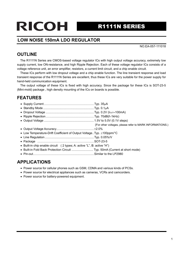
LOW NOISE 150m A LDO REGULATOR

NO.EA-057-111018

OUTLINE The R1111N Series are CMOS-based voltage regulator ICs with high output voltage accuracy, extremely low supply current, low ON-resistance, and high Ripple Rejection. Each of these voltage regulator ICs consists of a voltage reference unit, an error amplifier, resistors, a current limit circuit, and a chip enable circuit. These ICs perform with low dropout voltage and a chip enable function. The line transient response and load transient response of the R1111N Series are excellent, thus these ICs are very suitable for the power supply for hand-held communication equipment. The output voltage of these ICs is fixed with high accuracy. Since the package for these ICs is SOT-23-5 (Mini-mold) package , high density mounting of the ICs on boards is possible.

FEATURES • Supply Current ............................................................Typ. 35μA • Standby Mode .............................................................Typ. 0.1μA • Dropout Voltage ..........................................................Typ. 0.2V (IOUT=100m A) • Ripple Rejection..........................................................Typ. 70d B(f=1k Hz) • Output Voltage ............................................................1.5V to 5.0V (0.1V steps) (For other voltages, please refer to MARK INFORMATIONS.) • Output Voltage Accuracy.............................................±2.0% • Low Temperature-Drift Coefficient of Output Voltage..Typ. ±100ppm/°C • Line Regulation ...........................................................Typ. 0.05%/V • Package ....................................................................SOT-23-5 • Built-in chip enable circuit ( 2 types; A: active “L”, B: active “H”) • Built-in Fold Back Protection Circuit Typ. 50m A (Current at short mode) • Pin-out.........................................................................Similar to the LP2980

APPLICATIONS • Power source for cellular phones such as GSM, CDMA and various kinds of PCSs. • Power source for electrical appliances such as cameras, VCRs and camcorders. • Power source for battery-powered equipment.

Page Summary Contents For RICOH R1111N SERIES Owner's Manual and User Guide

Page 1 R1111N SERIES LOW NOISE 150m A LDO REGULATOR NO.EA-057-111018 OUTLINE The R1111N Series are CMOS-based voltage regulator ICs with high output voltage accuracy, extremely low supply current, low ON-res...
Page 2 BLOCK DIAGRAM R1111Nxx1A R1111Nxx1B VDD VOUT VDD VOUT Vref Vref Current Limit GNDCE Current Limit GNDCE SELECTION GUIDE The output voltage, the active type for the ICs can be selected at the user's re...
Page 3 PIN CONFIGURATION • SOT-23-5 (mark side) PIN DESCRIPTION • SOT-23-5 Pin No Symbol Pin Description 1 VDD Input Pin 2 GND Ground Pin 3 CE or CE Chip Enable Pin 4 NC No Connection 5 VOUT Output pin ABSOL...
Page 4 ELECTRICAL CHARACTERISTICS • R1111Nxx1A Topt=25°C Symbol Item Conditions Min. Typ. Max. Unit VOUT Output Voltage VIN = Set VOUT + 1V 1m A ≤ IOUT ≤ 30m A ×0.98 VOUT ×1.02 V IOUT Output Current Refer to...
Page 5 • R1111Nxx1B Topt=25°C Symbol Item Conditions Min. Typ. Max. Unit VOUT Output Voltage VIN = Set VOUT + 1V 1m A ≤ IOUT ≤ 30m A ×0.98 VOUT ×1.02 V IOUT Output Current Refer to the ELECTRICAL CHARACTERIS...
Page 6 ELECTRICAL CHARACTERISTICS by OUTPUT VOLTAGE Topt = 25°C Output Current Output Voltage IOUT (m A) VOUT (V) Condition Min. 1.5 ≤ VOUT ≤ 1.7 100 VIN - VOUT = 1.0V 1.8 ≤ VOUT ≤ 5.0 Topt = 25°C Dropout Vo...
Page 7 TEST CIRCUITS CE CE VDD VOUT VDD VOUT IN OUT IN OUT R1111Nxx1B Series R1111Nxx1B Series IOUT ISS 0.1μF GND 0.1μF GND Fig.1 Standard test Circuit Fig.2 Supply Current Test Circuit CE CE VDD VOUT VDD VO...
Page 8 ut pu t V ol ta ge (V ut pu t V ol ta ge (V ut pu t V ol ta ge (V TYPICAL CHARACTERISTICS 1) Output Voltage vs. Output Current R1111N181B R1111N301B Topt = 25°C Topt = 25°C VIN = 3.3V VIN = 2.1V Outpu...
Page 9 ro po ut ol ta ge IF ro po ut ol ta ge IF ut pu t V ol ta ge Topt = 25°C Topt = 25°C IOUT = 1m A 5.0 IOUT = 1m A 4.5 Intput Voltage VIN (V) Intput Voltage VIN (V) 3) Dropout Voltage vs. Output Current...
Page 10 up pl ur re nt IS μA ut pu t V ol ta ge (V ut pu t V ol ta ge (V 4) Output Voltage vs. Temperature R1111N181B R1111N301B VIN = 2.8V VIN = 4.0V IOUT = 30m A IOUT = 30m A Temperature Topt (°C) Temperatu...
Page 11 up pl ur re nt IS μA up pl ur re nt IS μA up pl ur re nt μA Topt = 25°C Topt = 25°C Intput Voltage VIN (V) Intput Voltage VIN (V) 6) Supply Current vs. Temperature R1111N181B R1111N301B VIN = 2.8V VIN...
Page 12 ip pl ej ec tio d B ip pl ej ec tio d B ro po ut ol ta ge IF (V 7) Dropout Voltage vs. Set Output Voltage R1111Nxx1B Topt = 25 0.8 IOUT = 150m A IOUT = 100m A IOUT = 50m A IOUT = 30m A IOUT = 10m A Se...
Page 13 ip pl ej ec tio (d ip pl ej ec tio (d ip pl ej ec tio (d VIN = 5.0VDC + 0.5Vp-p VIN = 5.0VDC + 0.5Vp-p COUT = tantal 1.0μF COUT = tantal 2.2μF IOUT= 1m A IOUT = 1m A IOUT = 30m A IOUT = 30m A IOUT = 5...
Page 14 ut pu t V ol ta ge (V ut pu t V ol ta ge (V ut pu t V ol ta ge (V 10) Input Transient Response IOUT=30m A tr=tf=5 μs COUT=Tantalum 1.0μF Input Voltage Output Voltage Time t (μs) IOUT=30m A tr=tf=5 μs ...
Page 15 11) Load Transient Response ut pu t V ol ta ge (V ut pu t V ol ta ge (V ut pu t V ol ta ge (V VIN=4V CIN=Tantalum 1μF COUT=Tantalum 1.0μF Output Current Output Voltage Time t (μs) VIN=4V CIN=Tantalum ...
Page 16 TECHNICAL NOTES When using these ICs, consider the following points: In these ICs, phase compensation is made for securing stable operation even if the load current is varied. For this purpose, be sur...
Page 17 ·Make VDD and GND lines sufficient. If their impedance is high, noise pick up or incorrect operation may result. ·Connect the capacitor with a capacitance of 1μF or more between VDD and GND as close a...
Page 18 1. The products and the product specifications described in this document are subject to change or discontinuation of production without notice for reasons such as improvement. Therefore, before decid...