Philips Semiconductors BU1706A Data Sheet
Summary
This datasheet provides complete specifications for the Philips BU1706A high-voltage high-speed switching NPN power transistor in a TO220AB plastic package, designed for high-frequency electronic lighting ballast applications. It details electrical characteristics, switching performance, thermal ratings, and safe operating area curves for power electronics design engineers.
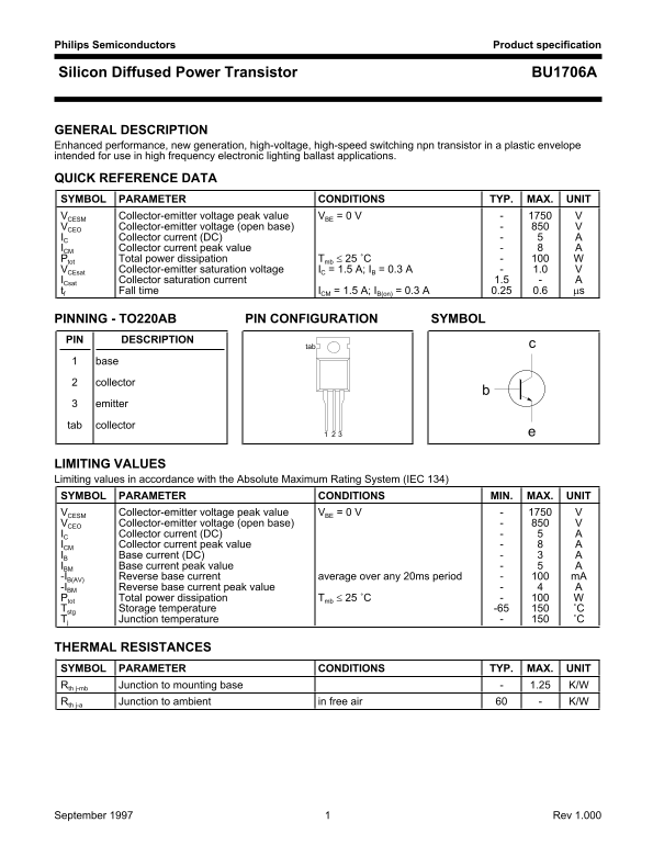
Page 1 Text Content
Philips Semiconductors Product specification
Silicon Diffused Power Transistor BU1706A
GENERAL DESCRIPTION Enhanced performance, new generation, high-voltage, high-speed switching npn transistor in a plastic envelope intended for use in high frequency electronic lighting ballast applications.
QUICK REFERENCE DATA SYMBOL PARAMETER CONDITIONS TYP. MAX. UNIT VCESM Collector-emitter voltage peak value VBE = 0 V VCEO Collector-emitter voltage (open base) IC Collector current (DC) ICM Collector current peak value Ptot Total power dissipation Tmb ≤ 25 ˚C VCEsat Collector-emitter saturation voltage IC = 1.5 A; IB = 0.3 A 1.0 ICsat Collector saturation current 1.5 tf Fall time ICM = 1.5 A; IB(on) = 0.3 A 0.25 0.6 µs
PINNING - TO220AB PIN CONFIGURATION SYMBOL PIN DESCRIPTION
collector emitter
tab collector
LIMITING VALUES Limiting values in accordance with the Absolute Maximum Rating System (IEC 134) SYMBOL PARAMETER CONDITIONS MIN. MAX. UNIT VCESM Collector-emitter voltage peak value VBE = 0 V VCEO Collector-emitter voltage (open base) IC Collector current (DC) ICM Collector current peak value IB Base current (DC) IBM Base current peak value -IB(AV) Reverse base current average over any 20ms period m A -IBM Reverse base current peak value Ptot Total power dissipation Tmb ≤ 25 ˚C Tstg Storage temperature -65 ˚C Tj Junction temperature ˚C
THERMAL RESISTANCES SYMBOL PARAMETER CONDITIONS TYP. MAX. UNIT Rth j-mb Junction to mounting base 1.25 K/W Rth j-a Junction to ambient in free air K/W
September 1997 Rev 1.000
Page Summary Contents For Philips Semiconductors BU1706A Data Sheet
Manual Details
| Brand | Philips |
|---|---|
| Pages | 7 |
| File Size | 76.69 KB |
| Published | June 17, 2026 |
Enter the captcha to get the download link:

Frequently Asked Questions
Can this transistor be used for life support applications?
No, the products are not designed for use in life support appliances or systems where malfunction can cause personal injury.
What is the maximum allowable collector current and voltage peak?
The peak limits are 8 A for Collector current (C_I) and up to 1750 V for the Collector-emitter voltage (V).
How must power dissipation be accounted for based on mounting conditions?
Power dissipation is governed by thermal resistances, specifically from Junction to Mounting Base ($R_{th j-mb}$) and Junction to Ambient air ($R_{th j-a}$).