PHILIPS PowerMOS Transistor BUK456-100B Data Sheet (1) User Manual
Summary
A high-voltage N-channel PowerMOS field-effect transistor designed for robust performance in demanding switching applications. This comprehensive technical manual provides electrical engineers and power electronics designers with all necessary specifications, making it critical for system design of SMPS, motor controls, welding units, and DC/AC converters. The resource details static and dynamic characteristics, defining limiting values, thermal resistance curves, and operational guidelines for building reliable high-power circuitry.
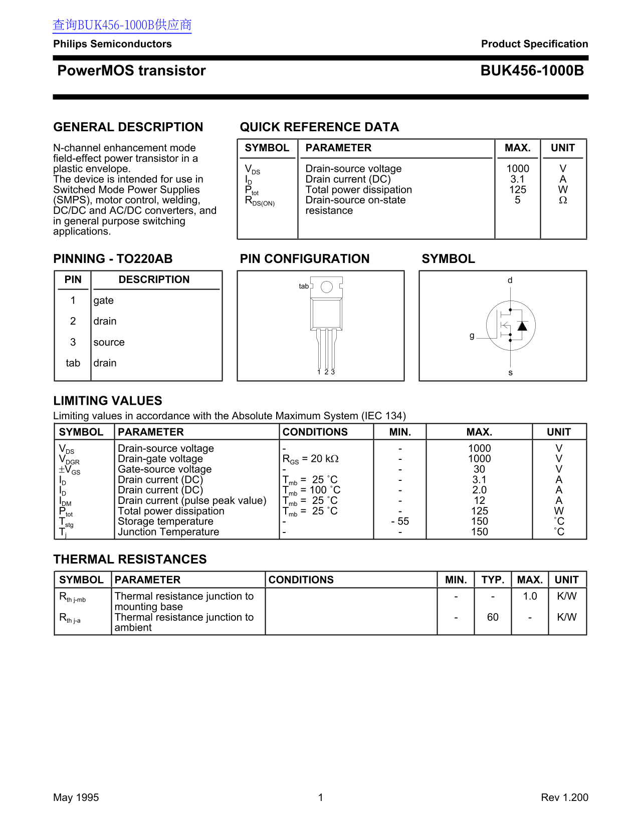
Page 1 Text Content
查询BUK456-1000B供应商 Philips Semiconductors Product Specification
Power MOS transistor BUK456-1000B
GENERAL DESCRIPTION QUICK REFERENCE DATA N-channel enhancement mode SYMBOL PARAMETER MAX. UNIT field-effect power transistor in a
plastic envelope. VDS Drain-source voltage
The device is intended for use in ID Drain current (DC) 3.1 Switched Mode Power Supplies Ptot Total power dissipation (SMPS), motor control, welding, RDS(ON) Drain-source on-state DC/DC and AC/DC converters, and resistance in general purpose switching applications.
PINNING - TO220AB PIN CONFIGURATION SYMBOL PIN DESCRIPTION
gate drain
source tab drain
LIMITING VALUES Limiting values in accordance with the Absolute Maximum System (IEC 134) SYMBOL PARAMETER CONDITIONS MIN. MAX. UNIT VDS Drain-source voltage VDGR Drain-gate voltage RGS = 20 kΩ ±VGS Gate-source voltage ID Drain current (DC) Tmb = 25 ˚C 3.1 ID Drain current (DC) Tmb = 100 ˚C 2.0 IDM Drain current (pulse peak value) Tmb = 25 ˚C Ptot Total power dissipation Tmb = 25 ˚C Tstg Storage temperature - 55 ˚C Tj Junction Temperature ˚C
THERMAL RESISTANCES SYMBOL PARAMETER CONDITIONS MIN. TYP. MAX. UNIT Rth j-mb Thermal resistance junction to 1.0 K/W
mounting base
Rth j-a Thermal resistance junction to K/W
ambient
May 1995 Rev 1.200
Page Summary Contents For PHILIPS PowerMOS Transistor BUK456-100B Data Sheet (1) User Manual
Manual Details
| Brand | Philips |
|---|---|
| Pages | 7 |
| File Size | 63.51 KB |
| Published | July 06, 2026 |
Enter the captcha to get the download link:

Frequently Asked Questions
What is the maximum drain-source voltage (V(DSS))?
The device has a Drain-source voltage of 1000 V.
Under what temperature must I confirm full drain current capability?
The continuous drain current maximum rating is 3.1 A at standard room temperature (25 °C).
Can this transistor be used in motor control applications?
Yes, it is intended for use in motor control and switching modes power supplies.
How do I calculate the thermal resistance check?
Use the Power Derating curve (Fig.4) to find the normalized thermal resistance required.