PHILIPS PowerMOS Transistor BUK445-200A Data Sheet
Summary
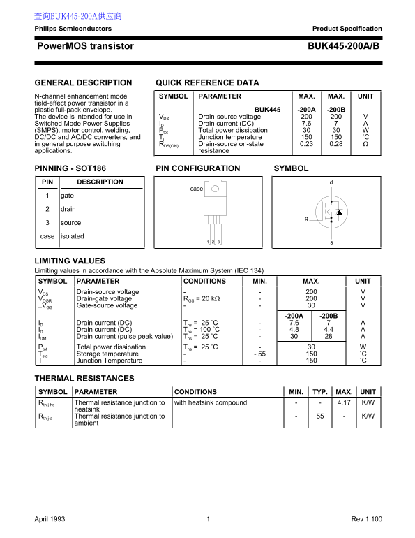
This Philips BUK445-200A and BUK445-200B PowerMOS N-channel enhancement mode field-effect transistor datasheet provides complete electrical specifications for switched mode power supply motor control welding and DC/DC converter applications. Covers 200V drain-source voltage rating with 7.6A continuous drain current capability at 25°C ambient temperature, 30W total power dissipation with SOT186 full-pack isolated plastic package enabling direct heatsink mounting without insulation washer requirem
Page 1 Text Content
查询BUK445-200A供应商 Philips Semiconductors Product Specification
Power MOS transistor BUK445-200A/B
GENERAL DESCRIPTION QUICK REFERENCE DATA N-channel enhancement mode SYMBOL PARAMETER MAX. MAX. UNIT field-effect power transistor in a plastic full-pack envelope. BUK445 -200A -200B
The device is intended for use in VDS Drain-source voltage
Switched Mode Power Supplies ID Drain current (DC) 7.6 (SMPS), motor control, welding, Ptot Total power dissipation DC/DC and AC/DC converters, and Tj Junction temperature ˚C
in general purpose switching RDS(ON) Drain-source on-state 0.23 0.28
applications. resistance
PINNING - SOT186 PIN CONFIGURATION SYMBOL PIN DESCRIPTION
gate drain
source case isolated
LIMITING VALUES Limiting values in accordance with the Absolute Maximum System (IEC 134) SYMBOL PARAMETER CONDITIONS MIN. MAX. UNIT VDS Drain-source voltage VDGR Drain-gate voltage RGS = 20 kΩ ±VGS Gate-source voltage
ID Drain current (DC) Ths = 25 ˚C 7.6 ID Drain current (DC) Ths = 100 ˚C 4.8 4.4 IDM Drain current (pulse peak value) Ths = 25 ˚C Ptot Total power dissipation Ths = 25 ˚C Tstg Storage temperature - 55 ˚C Tj Junction Temperature ˚C
THERMAL RESISTANCES SYMBOL PARAMETER CONDITIONS MIN. TYP. MAX. UNIT
Rth j-hs Thermal resistance junction to with heatsink compound 4.17 K/W heatsink
Rth j-a Thermal resistance junction to K/W
ambient
April 1993 Rev 1.100
Page Summary Contents For PHILIPS PowerMOS Transistor BUK445-200A Data Sheet
Manual Details
| Brand | Philips |
|---|---|
| Pages | 7 |
| File Size | 74.60 KB |
| Published | June 17, 2026 |
Enter the captcha to get the download link:

Frequently Asked Questions
What is the maximum continuous drain-source voltage?
The device has a maximum rated drain-source voltage ($V_{DS}$) of 200 V.
What are the intended applications for this PowerMOS transistor?
It is designed for use in SMPS, motor control, welding, and general DC/DC and AC/DC converters.
How should I identify the Gate, Drain, and Source pins?
The pin configuration lists Pin 1 as Gate (g), Pin 2 as Drain (d), and Pin 3 as Source (s).
What is the maximum rated total power dissipation?
The maximum total power dissipation ($P_{Total}$) must not exceed 30 W.
Are these devices suitable for use in life support applications?
No, these products are not designed for use in life support appliances or systems.