Philips PowerMOS Transistor BUK454-60H Data Handbook
Summary
The BUK454-60H is a high-power N-channel PowerMOS transistor engineered for reliable performance in demanding power applications. It is essential for building robust electronics, including SMPS units, motor controllers, welding equipment, and DC/DC converters. This datasheet provides comprehensive technical specifications, detailing absolute maximum ratings, thermal resistances, dynamic characteristics, and detailed operating limits (up to 60V). Designed specifically for electrical engineers and hardware designers requiring accurate, professional-grade data for high-power switching circuit development.
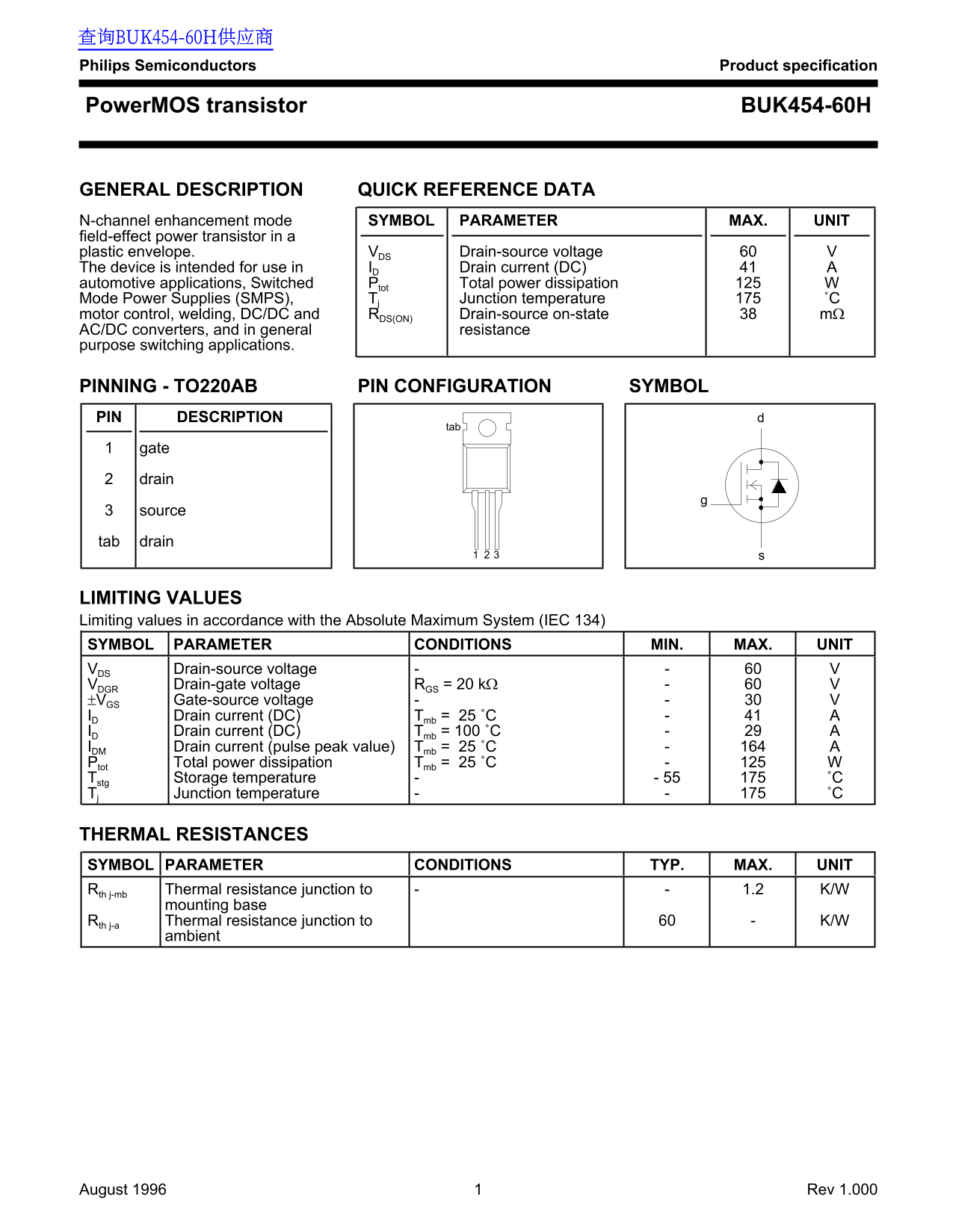
Page 1 Text Content
查询BUK454-60H供应商 Philips Semiconductors Product specification
Power MOS transistor BUK454-60H
GENERAL DESCRIPTION QUICK REFERENCE DATA N-channel enhancement mode SYMBOL PARAMETER MAX. UNIT field-effect power transistor in a
plastic envelope. VDS Drain-source voltage
The device is intended for use in ID Drain current (DC) automotive applications, Switched Ptot Total power dissipation Mode Power Supplies (SMPS), Tj Junction temperature ˚C motor control, welding, DC/DC and RDS(ON) Drain-source on-state mΩ AC/DC converters, and in general resistance purpose switching applications.
PINNING - TO220AB PIN CONFIGURATION SYMBOL PIN DESCRIPTION
gate drain
source tab drain
LIMITING VALUES Limiting values in accordance with the Absolute Maximum System (IEC 134) SYMBOL PARAMETER CONDITIONS MIN. MAX. UNIT VDS Drain-source voltage VDGR Drain-gate voltage RGS = 20 kΩ ±VGS Gate-source voltage ID Drain current (DC) Tmb = 25 ˚C ID Drain current (DC) Tmb = 100 ˚C IDM Drain current (pulse peak value) Tmb = 25 ˚C Ptot Total power dissipation Tmb = 25 ˚C Tstg Storage temperature - 55 ˚C Tj Junction temperature ˚C
THERMAL RESISTANCES SYMBOL PARAMETER CONDITIONS TYP. MAX. UNIT Rth j-mb Thermal resistance junction to 1.2 K/W
mounting base
Rth j-a Thermal resistance junction to K/W
ambient
August 1996 Rev 1.000
Page Summary Contents For Philips PowerMOS Transistor BUK454-60H Data Handbook
Manual Details
| Brand | Philips |
|---|---|
| Pages | 7 |
| File Size | 49.81 KB |
| Published | July 15, 2026 |
Enter the captcha to get the download link:

Frequently Asked Questions
What is the maximum allowed continuous drain current at 25°C?
The maximum rating is 41 A (I Drain current (DC) at T = 25˚C).
Is this device safe for use in life support appliances?
No, these products are not designed for use in life support systems. Use is at the customer’s own risk.
What must be done if the device is exposed to limiting values for extended periods?
Exposure may affect device reliability, and these ratings are stress only.
What are the typical limits for gate-source voltage?
The required Gate-source voltage range is -30 V to 30 V (GS).