Panasonic 2SK123 Silicon N-Channel Junction FET Specifications and User Guide
Summary
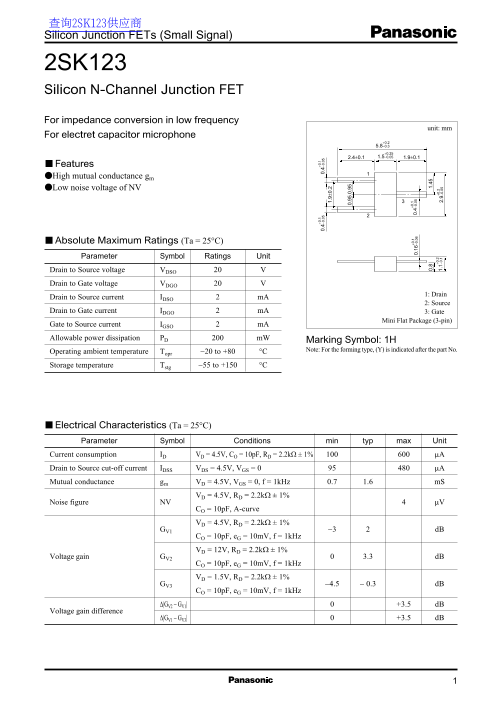
This datasheet describes the Panasonic 2SK123 silicon N-channel junction FET in a mini flat 3-pin package, designed for impedance conversion in low-frequency applications and electret condenser microphone circuits. Key performance characteristics include high mutual conductance of 1.6mS typical at 4.5V drain voltage, and low noise voltage of 4μV typical under specified measurement conditions with 10pF output capacitance and A-curve weighting. Drain-to-source cutoff current at zero gate voltage i
Page 1 Text Content
查询2SK123供应商 Silicon Junction FETs (Small Signal)
2SK123 Silicon N-Channel Junction FET For impedance conversion in low frequency
unit: mm
For electret capacitor microphone
Features High mutual conductance gm Low noise voltage of NV
Absolute Maximum Ratings (Ta = 25°C) Parameter Symbol Ratings Unit Drain to Source voltage VDSO Drain to Gate voltage VDGO
1: Drain
Drain to Source current IDSO m A
2: Source
Drain to Gate current IDGO m A 3: Gate
Mini Flat Package (3-pin) .1 .1 0. 4+0 −0 .0 0. 4+0 −0 .0
Gate to Source current IGSO m A
Allowable power dissipation PD m W
Marking Symbol: 1H
Note: For the forming type, (Y) is indicated after the part No. 0. 0.
Operating ambient temperature Topr −20 to +80 °C
Storage temperature Tstg −55 to +150 °C
Electrical Characteristics (Ta = 25°C)
0. 1. .2 .2 Parameter Symbol Conditions min typ max Unit 1. 1+0 −0 .1 2. 9+0 −0 .0
Current consumption ID VD = 4.5V, CO = 10p F, RD = 2.2kΩ ± 1% µA Drain to Source cut-off current IDSS VDS = 4.5V, VGS = 0 µA Mutual conductance gm VD = 4.5V, VGS = 0, f = 1k Hz 0.7 1.6 m S
VD = 4.5V, RD = 2.2kΩ ± 1%
Noise figure NV µV
CO = 10p F, A-curve VD = 4.5V, RD = 2.2kΩ ± 1%
GV1 −3 d B
CO = 10p F, e G = 10m V, f = 1k Hz VD = 12V, RD = 2.2kΩ ± 1%
Voltage gain GV2 3.3 d B
CO = 10p F, e G = 10m V, f = 1k Hz VD = 1.5V, RD = 2.2kΩ ± 1%
GV3 −4.5 − 0.3 d B
CO = 10p F, e G = 10m V, f = 1k Hz
∆|GV2 − GV1| +3.5 d B
Voltage gain difference
∆|GV1 − GV3| +3.5 d B
Page Summary Contents For Panasonic 2SK123 Silicon N-Channel Junction FET Specifications and User Guide
Manual Details
| Brand | Panasonic |
|---|---|
| Pages | 2 |
| File Size | 25.98 KB |
| Published | June 18, 2026 |
Enter the captcha to get the download link:

Frequently Asked Questions
What is the safe operating temperature range for this device?
The operating ambient temperature (T_opr) ranges from -20 to +80 °C. The storage temperature (T_stg) is -55 to +150 °C.
Are there specific power limits I should be aware of?
The allowable power dissipation (P) for the device is 200 mW.
How does the mutual conductance (g_m) measure performance?
Mutual conductance (g_m) is measured in mS and indicates electrical performance under specific voltage and frequency conditions.
What are the maximum ratings for voltages?
The absolute maximum ratings include a Drain to Source voltage of 20 V, a Drain to Gate voltage of 20 V, and an allowable power dissipation (P) of 200 mW.