Panasonic 2SK1103 Silicon N-Channel Junction FET User Guide and Manual
Summary
A highly reliable Silicon Junction FET designed for efficient, small signal switching applications. This component features low ON-resistance and exceptional low-noise characteristics, making it ideal for sophisticated power electronics designs. The manual provides comprehensive technical specifications essential for circuit development. It details absolute maximum operational ratings, critical electrical parameters (including $R_{DS(on)}$ and capacitances), and performance metrics across varying temperature ranges, ensuring precise integration into complex miniature switching units.
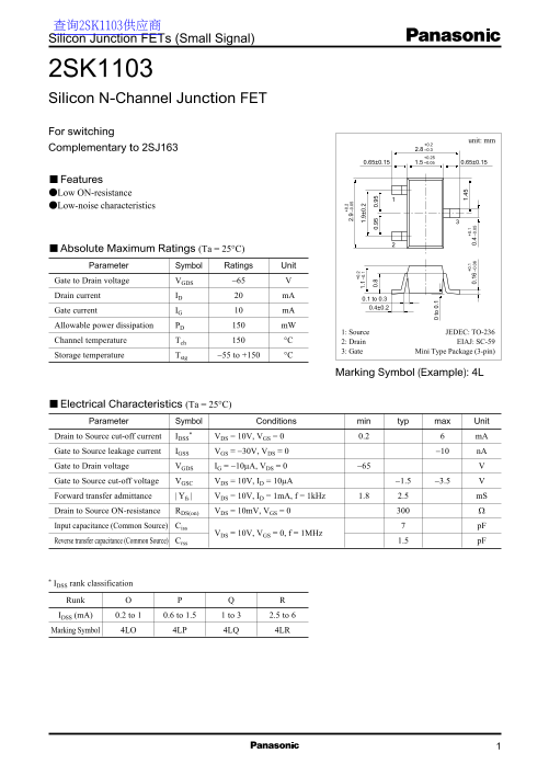
Page 1 Text Content
查询2SK1103供应商 Silicon Junction FETs (Small Signal)
2SK1103 Silicon N-Channel Junction FET For switching
unit: mm
Complementary to 2SJ163 2.8 –0.3
Features Low ON-resistance Low-noise characteristics
Absolute Maximum Ratings (Ta = 25°C) Parameter Symbol Ratings Unit Gate to Drain voltage VGDS −65 Drain current ID m A
0.1 to 0.3 0.4±0.2
Gate current IG m A Allowable power dissipation PD m W
1: Source JEDEC: TO-236
Channel temperature Tch °C 2: Drain EIAJ: SC-59
0. 3: Gate Mini Type Package (3-pin) 2. –0 .0
Storage temperature Tstg −55 to +150 °C 0.
Marking Symbol (Example): 4L 0.
Electrical Characteristics (Ta = 25°C) Parameter Symbol Conditions min typ max Unit
Drain to Source cut-off current IDSS VDS = 10V, VGS = 0 0.2 to .1 m A
Gate to Source leakage current IGSS VGS = −30V, VDS = 0 −10 n A
Gate to Drain voltage VGDS IG = −10µA, VDS = 0 −65 1.
Gate to Source cut-off voltage VGSC VDS = 10V, ID = 10µA −1.5 −3.5 Forward transfer admittance | Yfs | VDS = 10V, ID = 1m A, f = 1k Hz 1.8 2.5 m S Drain to Source ON-resistance RDS(on) VDS = 10m V, VGS = 0
Input capacitance (Common Source) Ciss p F
VDS = 10V, VGS = 0, f = 1MHz
Reverse transfer capacitance (Common Source) Crss 1.5 p F
* IDSS rank classification
IDSS (m A) 0.2 to 1 0.6 to 1.5 1 to 3 2.5 to 6
Marking Symbol 4LO 4LP 4LQ 4LR
Page Summary Contents For Panasonic 2SK1103 Silicon N-Channel Junction FET User Guide and Manual
Manual Details
| Brand | Panasonic |
|---|---|
| Pages | 2 |
| File Size | 27.44 KB |
| Published | June 16, 2026 |
Enter the captcha to get the download link:

Frequently Asked Questions
What complementary component works with the 2SK1103?
It is listed as being complementary to model 2SJ163.
What are the maximum electrical ratings for drain current and dissipation?
The continuous Drain current (I_D) is rated at 20 mA, with an allowable power dissipation (P) of 150 mW D.
Can this component handle extreme temperatures?
Yes. The storage temperature range (T_stg) for the package is -55 to +150 degrees Celsius.
What package type does the 2SK1103 utilize?
The component uses a TO-236 package type, meeting JEDEC standards.