ON Semiconductor CS1112 Quad Power Output Driver Data Sheet User Manual
Summary
The CS1112 is a sophisticated quad power output driver IC designed specifically for reliable performance in demanding automotive environments. It features four protected low-side drivers capable of managing inductive and resistive loads while providing extensive fault protection (including overcurrent, open load, and transient voltage detection). This manual serves as a comprehensive technical guide, detailing the SPI interface, operational parameters, and diagnostic status reporting. It is essential for electrical engineers developing complex automotive control systems requiring maximum power efficiency and safety assurance.
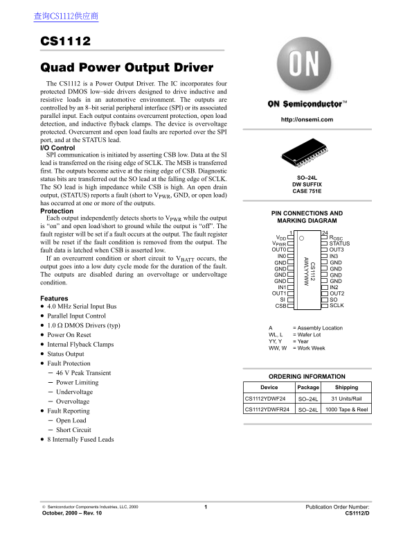
Page 1 Text Content
查询CS1112供应商
CS1112
Quad Power Output Driver The CS1112 is a Power Output Driver. The IC incorporates four protected DMOS low–side drivers designed to drive inductive and resistive loads in an automotive environment. The outputs are
controlled by an 8–bit serial peripheral interface (SPI) or its associated parallel input. Each output contains overcurrent protection, open load
http://onsemi.com
detection, and inductive flyback clamps. The device is overvoltage protected. Overcurrent and open load faults are reported over the SPI port, and at the STATUS lead. I/O Control SPI communication is initiated by asserting CSB low. Data at the SI lead is transferred on the rising edge of SCLK. The MSB is transferred first. The outputs become active at the rising edge of CSB. Diagnostic
status bits are transferred out the SO lead at the falling edge of SCLK. SO–24L DW SUFFIX
The SO lead is high impedance while CSB is high. An open drain
CASE 751E
output, (STATUS) reports a fault (short to VPWR, GND, or open load) has occurred at one or more of the outputs. Protection
PIN CONNECTIONS AND
Each output independently detects shorts to VPWR while the output
MARKING DIAGRAM
is “on” and open load/short to ground while the output is “off”. The fault register will be set if a fault occurs at the output. The fault register
VDD ROSC
will be reset if the fault condition is removed from the output. The VPWR STATUS
fault data is latched when CSB is asserted low. OUT0 OUT3 IN0 IN3
If an overcurrent condition or short circuit to VBATT occurs, the
GND GND
output goes into a low duty cycle mode for the duration of the fault.
GND GND
The outputs are disabled during an overvoltage or undervoltage GND GND
condition. GND GND IN1 IN2 OUT1 OUT2
Features SI SO
4.0 MHz Serial Input Bus CSB SCLK
Parallel Input Control 1.0 Ω DMOS Drivers (typ)
= Assembly Location
Power On Reset WL, L = Wafer Lot YY, Y = Year
Internal Flyback Clamps
WW, W = Work Week
Status Output Fault Protection 46 V Peak Transient
ORDERING INFORMATION
Power Limiting
Device Package Shipping
Undervoltage
CS1112YDWF24 SO–24L 31 Units/Rail
Overvoltage
Fault Reporting CS1112YDWFR24 SO–24L 1000 Tape & Reel
Open Load Short Circuit 8 Internally Fused Leads
Semiconductor Components Industries, LLC, 2000 Publication Order Number: October, 2000 – Rev. 10 CS1112/D
Page Summary Contents For ON Semiconductor CS1112 Quad Power Output Driver Data Sheet User Manual
Manual Details
| Brand | QUAD |
|---|---|
| Pages | 12 |
| File Size | 96.76 KB |
| Published | May 27, 2026 |
Enter the captcha to get the download link:

Frequently Asked Questions
What types of electrical loads can the CS1112 operate with?
It is designed to drive both inductive and resistive loads in an automotive environment.
How are faults like overcurrent or open load detected by the chip?
These faults are reported over both the SPI port and monitored via the STATUS lead.
What needs to happen to send command data through the serial interface?
I/O Control communication is initiated by asserting the CSB pin low.
How does the device prevent damage from voltage surges?
The device includes overvoltage protection and utilizes internal flyback clamps for safety.