MOTOROLA MTW16N40E Data Sheet
Summary
A robust N-Channel Power MOSFET engineered for high-speed, high-voltage switching up to 400V. This device features advanced termination technology for enhanced performance and reliability in critical applications. The corresponding datasheet provides comprehensive technical specifications, including electrical characteristics, thermal limits, and detailed dynamic data essential for reliable circuit design. It is the ideal component for engineers specifying designs for power supplies, DC-DC converters, and PWM motor control systems.
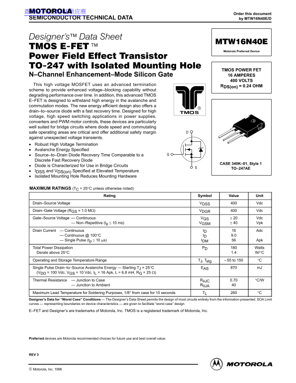
Page 1 Text Content
查询MTW16N40E供应商
Order this document
SEMICONDUCTOR TECHNICAL DATA by MTW16N40E/D
Motorola Preferred Device
TMOS POWER FET
N–Channel Enhancement–Mode Silicon Gate 16 AMPERES
400 VOLTS
This high voltage MOSFET uses an advanced termination
RDS(on) = 0.24 OHM
scheme to provide enhanced voltage–blocking capability without degrading performance over time. In addition, this advanced TMOS E–FET is designed to withstand high energy in the avalanche and commutation modes. The new energy efficient design also offers a drain–to–source diode with a fast recovery time. Designed for high voltage, high speed switching applications in power supplies, converters and PWM motor controls, these devices are particularly well suited for bridge circuits where diode speed and commutating safe operating areas are critical and offer additional safety margin against unexpected voltage transients. Robust High Voltage Termination Avalanche Energy Specified Source–to–Drain Diode Recovery Time Comparable to a Discrete Fast Recovery Diode
CASE 340K–01, Style 1
Diode is Characterized for Use in Bridge Circuits
TO–247AE
IDSS and VDS(on) Specified at Elevated Temperature Isolated Mounting Hole Reduces Mounting Hardware
MAXIMUM RATINGS (TC = 25°C unless otherwise noted)
Rating Symbol Value Unit
Drain–Source Voltage VDSS Vdc Drain–Gate Voltage (RGS = 1.0 MΩ) VDGR Vdc Gate–Source Voltage — Continuous VGS Vdc
— Non–Repetitive (tp ≤ 10 ms) VGSM Vpk
Drain Current — Continuous ID Adc
— Continuous @ 100°C ID 9.0 — Single Pulse (tp ≤ 10 µs) IDM Apk
Total Power Dissipation PD Watts Derate above 25°C 1.4 W/°C Operating and Storage Temperature Range TJ, Tstg –55 to 150 °C Single Pulse Drain–to–Source Avalanche Energy — Starting TJ = 25°C EAS m J (VDD = 100 Vdc, VGS = 10 Vdc, IL = 16 Apk, L = 6.8 m H, RG = 25 Ω) Thermal Resistance — Junction to Case RθJC 0.70 °C/W
— Junction to Ambient RθJA
Maximum Lead Temperature for Soldering Purposes, 1/8″ from case for 10 seconds TL °C Designer’s Data for “Worst Case” Conditions — The Designer’s Data Sheet permits the design of most circuits entirely from the information presented. SOA Limit curves — representing boundaries on device characteristics — are given to facilitate “worst case” design. E–FET and Designer’s are trademarks of Motorola, Inc. TMOS is a registered trademark of Motorola, Inc.
Preferred devices are Motorola recommended choices for future use and best overall value.
REV 3
1Motorola TMOS Power MOSFET Transistor Device Data
Motorola, Inc. 1996
Page Summary Contents For MOTOROLA MTW16N40E Data Sheet
Manual Details
| Brand | Motorola |
|---|---|
| Pages | 8 |
| File Size | 218.46 KB |
| Published | June 01, 2026 |
Enter the captcha to get the download link:

Frequently Asked Questions
What types of applications is this power FET best suited for?
It is designed for high voltage, high speed switching in applications such as power supplies, converters, and PWM motor controls.
What does the device offer for superior performance in bridge circuits?
It features a source-to-drain diode recovery time comparable to a discrete fast recovery diode, offering additional safety margin against transient voltage spikes.
What are the specified maximum ratings for voltage and current (T=25°C)?
The maximum drain–source voltage is 400 Vdc, and the continuous drain current (Id) at 100°C is 9.0 Adc.
How reliable is the device during high-energy switching events?
It is designed to withstand high energy in both avalanche and commutation modes, with a specified Avalanche Energy (EAS) of 870 mJ.