Motorola DTA143EE Data Sheet
Summary
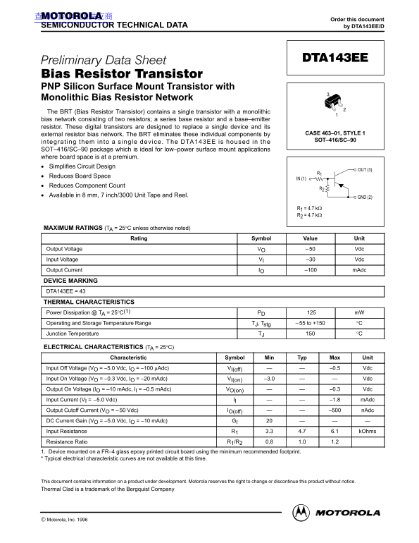
This highly compact PNP Silicon Surface Mount Transistor is engineered as a Bias Resistor Transistor (BRT), integrating multiple resistors into a single SOT–416/SC–90 package. It allows designers to drastically simplify circuit boards and conserve space by eliminating the need for external resistor networks. This technical manual provides critical specifications, including electrical characteristics, maximum ratings, power dissipation calculations, recommended footprints, and detailed soldering procedures required for reliable low-power, surface mount applications.
Page 1 Text Content
查询DTA143EE供应商
Order this document
SEMICONDUCTOR TECHNICAL DATA by DTA143EE/D
PNP Silicon Surface Mount Transistor with Monolithic Bias Resistor Network The BRT (Bias Resistor Transistor) contains a single transistor with a monolithic bias network consisting of two resistors; a series base resistor and a base–emitter resistor. These digital transistors are designed to replace a single device and its
external resistor bias network. The BRT eliminates these individual components by CASE 463–01, STYLE 1 SOT–416/SC–90
integrat ing them into a s ingle dev ice. The DTA143EE is housed in the SOT–416/SC–90 package which is ideal for low–power surface mount applications where board space is at a premium. Simplifies Circuit Design
OUT (3)
Reduces Board Space
IN (1)
Reduces Component Count
Available in 8 mm, 7 inch/3000 Unit Tape and Reel.
GND (2)
MAXIMUM RATINGS (TA = 25°C unless otherwise noted)
Rating Symbol Value Unit
Output Voltage VO –50 Vdc Input Voltage VI –30 Vdc Output Current IO –100 m Adc
DEVICE MARKING DTA143EE = 43 THERMAL CHARACTERISTICS Power Dissipation @ TA = 25°C(1) PD *125 m W Operating and Storage Temperature Range TJ, Tstg –55 to +150 °C Junction Temperature TJ °C
ELECTRICAL CHARACTERISTICS (TA = 25°C)
Characteristic Symbol Min Typ Max Unit
Input Off Voltage (VO = –5.0 Vdc, IO = –100 µAdc) VI(off) –0.5 Vdc Input On Voltage (VO = –0.3 Vdc, IO = –20 m Adc) VI(on) –3.0 Vdc Output On Voltage (IO = –10 m Adc, II = –0.5 m Adc) VO(on) –0.3 Vdc Input Current (VI = –5.0 Vdc) II –1.8 m Adc Output Cutoff Current (VO = –50 Vdc) IO(off) –500 n Adc DC Current Gain (VO = –5.0 Vdc, IO = –10 m Adc) GI Input Resistance R1 3.3 4.7 6.1 k Ohms Resistance Ratio R1/R2 0.8 1.0 1.2 1. Device mounted on a FR–4 glass epoxy printed circuit board using the minimum recommended footprint. * Typical electrical characteristic curves are not available at this time.
This document contains information on a product under development. Motorola reserves the right to change or discontinue this product without notice. Thermal Clad is a trademark of the Bergquist Company
Motor la, Inc. 1996 1Motorola Small–Signal Transistors, FETs and Diodes Device Data
Page Summary Contents For Motorola DTA143EE Data Sheet
Manual Details
| Brand | Motorola |
|---|---|
| Pages | 4 |
| File Size | 94.41 KB |
| Published | May 31, 2026 |
Enter the captcha to get the download link:

Frequently Asked Questions
What is the purpose of the DTA143EE device?
It's a PNP Silicon Surface Mount Transistor with a monolithic bias resistor network, eliminating external components for simplified circuit design.
What are the mandatory soldering precautions for this device?
Preheat, avoid excessive temperatures (over 260°C for >10 seconds), cool naturally for at least three minutes, and keep the maximum temperature gradient at 5°C or less.
How is power dissipation calculated for surface mount applications?
P = T - T J(max) A / R θJA. For 125 mW, the recommended footprint is shown in the datasheet.
What specific physical dimensions are required for mounting?
The minimum recommended footprints generally feature a geometry of 0.5 mm (3x) and standard soldering pattern dimensions provided in the manual.