MOTOROLA MRF175LU Data Sheet
Summary
These high-power N-Channel RF MOSFETs are engineered for demanding solid-state transmitters used in broadband communication, including FM broadcast and TV channel systems up to 400 MHz. This technical data sheet provides comprehensive specifications, covering maximum ratings, electrical characteristics, and functional performance of models MRF175LU and MRF175LV. It is essential documentation for RF engineers designing reliable, high-efficiency equipment requiring robust power handling capabilities.
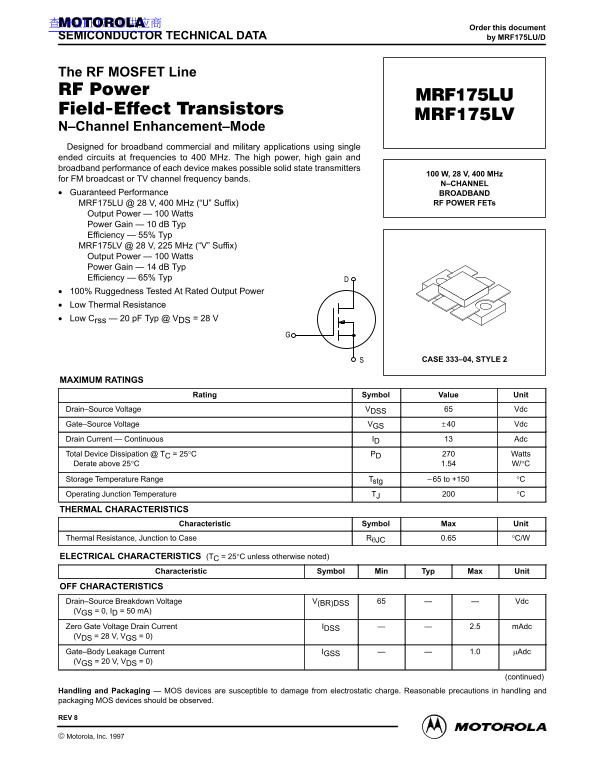
Page 1 Text Content
查询MRF175LU供应商
Order this document
SEMICONDUCTOR TECHNICAL DATA by MRF175LU/D
The RF MOSFET Line
N–Channel Enhancement–Mode Designed for broadband commercial and military applications using single ended circuits at frequencies to 400 MHz. The high power, high gain and broadband performance of each device makes possible solid state transmitters
100 W, 28 V, 400 MHz
for FM broadcast or TV channel frequency bands.
N–CHANNEL
Guaranteed Performance BROADBAND
MRF175LU @ 28 V, 400 MHz (“U” Suffix) RF POWER FETs
Output Power — 100 Watts Power Gain — 10 d B Typ Efficiency — 55% Typ MRF175LV @ 28 V, 225 MHz (“V” Suffix) Output Power — 100 Watts Power Gain — 14 d B Typ Efficiency — 65% Typ 100% Ruggedness Tested At Rated Output Power Low Thermal Resistance Low Crss — 20 p F Typ @ VDS = 28 V
CASE 333–04, STYLE 2
MAXIMUM RATINGS
Rating Symbol Value Unit
Drain–Source Voltage VDSS Vdc Gate–Source Voltage VGS ±40 Vdc Drain Current — Continuous ID Adc Total Device Dissipation @ TC = 25°C PD Watts Derate above 25°C 1.54 W/°C Storage Temperature Range Tstg –65 to +150 °C Operating Junction Temperature TJ °C
THERMAL CHARACTERISTICS
Characteristic Symbol Max Unit
Thermal Resistance, Junction to Case RθJC 0.65 °C/W
ELECTRICAL CHARACTERISTICS (TC = 25°C unless otherwise noted)
Characteristic Symbol Min Typ Max Unit
OFF CHARACTERISTICS Drain–Source Breakdown Voltage V(BR)DSS Vdc (VGS = 0, ID = 50 m A) Zero Gate Voltage Drain Current IDSS 2.5 m Adc (VDS = 28 V, VGS = 0) Gate–Body Leakage Current IGSS 1.0 µAdc (VGS = 20 V, VDS = 0)
(continued)
Handling and Packaging — MOS devices are susceptible to damage from electrostatic charge. Reasonable precautions in handling and packaging MOS devices should be observed.
REV 8
Motorola, Inc. 1997 MRF175LU MRF175LVMOTOROLA RF DEVICE DATA
Page Summary Contents For MOTOROLA MRF175LU Data Sheet
Manual Details
| Brand | Motorola |
|---|---|
| Pages | 8 |
| File Size | 141.03 KB |
| Published | June 02, 2026 |
Enter the captcha to get the download link:

Frequently Asked Questions
What is the primary difference between MRF175LU and MRF175LV?
The 'U' suffix (MRF175LU) is designed for 400 MHz, while the 'V' suffix (MRF175LV) is designed for 225 MHz.
What are the safe handling precautions for these MOS devices?
MOS devices are sensitive to damaging electrostatic charge; reasonable precautions must be taken during handling and packaging.
What is the maximum rated output power for these FETs?
Both models can handle a maximum specified output power of 100 Watts at 28 V.