Motorola MCM69R736A•MCM69R818A Data Sheet
Summary
Engineered for critical, high-speed memory needs, this synchronous SRAM is a high-performance 4 Mbit device ideal for telecommunication switches, ATM networks, and robust secondary cache applications. Professionals and system designers rely on this detailed manual source for everything required to integrate the component. It provides comprehensive technical specifications, functional block diagrams, precise pin assignments, and advanced operational guidance—including support for HSTL inputs and programmable output impedance—ensuring optimal performance in demanding electronic designs.
Page 1 Text Content
查询MCM69R736A供应商
Order this document
SEMICONDUCTOR TECHNICAL DATA by MCM69R736A/D
MCM69R736A
Advance Information
MCM69R818A
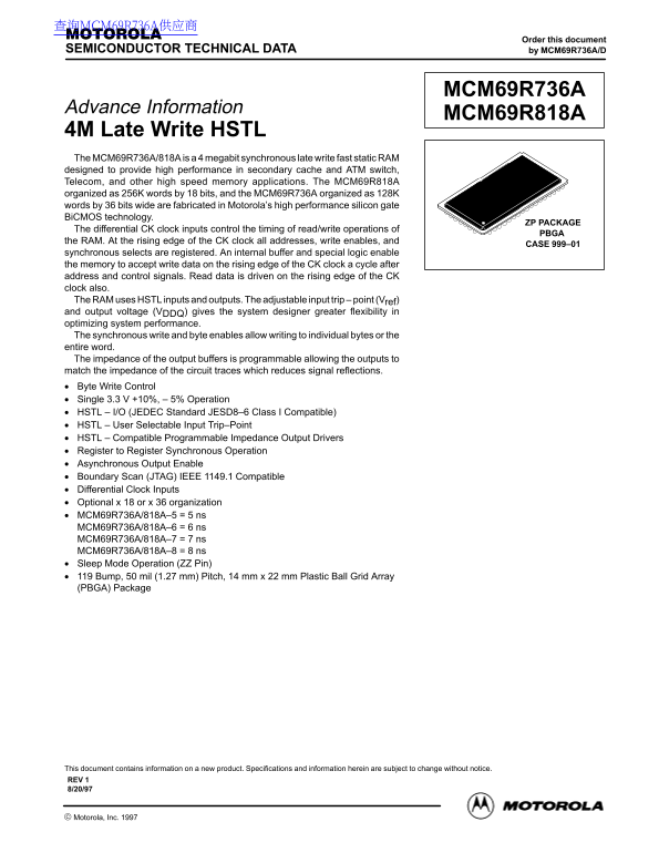
4M Late Write HSTL The MCM69R736A/818A is a 4 megabit synchronous late write fast static RAM designed to provide high performance in secondary cache and ATM switch, Telecom, and other high speed memory applications. The MCM69R818A organized as 256K words by 18 bits, and the MCM69R736A organized as 128K words by 36 bits wide are fabricated in Motorola’s high performance silicon gate Bi CMOS technology.
ZP PACKAGE
The differential CK clock inputs control the timing of read/write operations of
the RAM. At the rising edge of the CK clock all addresses, write enables, and
CASE 999–01
synchronous selects are registered. An internal buffer and special logic enable the memory to accept write data on the rising edge of the CK clock a cycle after address and control signals. Read data is driven on the rising edge of the CK clock also. The RAM uses HSTL inputs and outputs. The adjustable input trip – point (Vref) and output voltage (VDDQ) gives the system designer greater flexibility in optimizing system performance. The synchronous write and byte enables allow writing to individual bytes or the entire word. The impedance of the output buffers is programmable allowing the outputs to match the impedance of the circuit traces which reduces signal reflections. Byte Write Control Single 3.3 V +10%, – 5% Operation HSTL – I/O (JEDEC Standard JESD8–6 Class I Compatible) HSTL – User Selectable Input Trip–Point HSTL – Compatible Programmable Impedance Output Drivers Register to Register Synchronous Operation Asynchronous Output Enable Boundary Scan (JTAG) IEEE 1149.1 Compatible Differential Clock Inputs Optional x 18 or x 36 organization MCM69R736A/818A–5 = 5 ns MCM69R736A/818A–6 = 6 ns MCM69R736A/818A–7 = 7 ns MCM69R736A/818A–8 = 8 ns Sleep Mode Operation (ZZ Pin) 119 Bump, 50 mil (1.27 mm) Pitch, 14 mm x 22 mm Plastic Ball Grid Array (PBGA) Package
This document contains information on a new product. Specifications and information herein are subject to change without notice. REV 1 8/20/97
MOTOROLA FAST SRAM Motorola, Inc. 1997 MCM69R736A•MCM69R818A
Page Summary Contents For Motorola MCM69R736A•MCM69R818A Data Sheet
Manual Details
| Brand | Motorola |
|---|---|
| Pages | 20 |
| File Size | 229.76 KB |
| Published | May 31, 2026 |
Enter the captcha to get the download link:

Frequently Asked Questions
How is signal reflection minimized on the output data lines?
The output buffers have programmable impedance, which allows them to match the impedance of the circuit traces.
What standard does the device support for testing communication interfaces?
The RAM supports Boundary Scan (JTAG) and is compatible with IEEE 1149.1.
How can I put the memory into a low-power state?
Activate the ZZ pin to put the module into Sleep Mode Operation.
At what point are addresses and control signals registered during operation?
All addresses, write enables, and synchronous selects are registered on the rising edge of the CK clock.