MOTOROLA MC74F195 Data Sheet
Summary
This versatile component is a high-speed 4-Bit Parallel Access Shift Register (Schottky TTL), designed for robust shifting, counting, and storage applications. It facilitates flexible data transfers—including parallel load, shift right, and left operations—at very high speeds using synchronized clock transitions. The comprehensive documentation includes detailed logic diagrams, operational function tables, and precise electrical specifications (timing characteristics, voltage, current limits). This manual is essential for electronics engineers and hardware designers implementing reliable, high-performance digital circuits.
Page 1 Text Content
查询MC74F195供应商
MC74F195
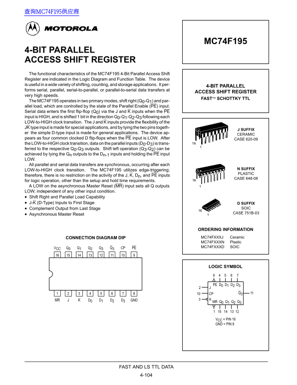
4-BIT PARALLEL ACCESS SHIFT REGISTER The functional characteristics of the MC74F195 4-Bit Parallel Access Shift Register are indicated in the Logic Diagram and Function Table. The device is useful in a wide variety of shifting, counting, and storage applications. It per-
4-BIT PARALLEL
forms serial, parallel, serial-to-parallel, or parallel-to-serial data transfers at
ACCESS SHIFT REGISTER
very high speeds.
FAST SCHOTTKY TTL
The MC74F195 operates in two primary modes, shift right (Q0-Q1) and par- allel load, which are controlled by the state of the Parallel Enable (PE) input. Serial data enters the first flip-flop (Q0) via the J and K inputs when the PE input is HIGH, and is shifted 1 bit in the direction Q0-Q1-Q2-Q3 following each LOW-to-HIGH clock transition. The J and K inputs provide the flexibility of the JK type input is made for special applications, and by tying the two pins togeth-
J SUFFIX
er the simple D-type input is made for general applications. The device ap-
CERAMIC
pears as four common clocked D flip-flops when the PE input is LOW. After
CASE 620-09
the LOW-to-HIGH clock transition, data on the parallel inputs (D0-D3) is trans- ferred to the respective Q0-Q3 outputs. Shift left operation (Q3-Q2) can be achieved by tying the Qn outputs to the Dn-1 inputs and holding the PE input LOW. All parallel and serial data transfers are synchronous, occurring after each
N SUFFIX
LOW-to-HIGH clock transition. The MC74F195 utilizes edge-triggering;
PLASTIC
therefore, there is no restriction on the activity of the J, K, Dn, and PE inputs
CASE 648-08
for logic operation, other than the setup and hold time requirements. A LOW on the asynchronous Master Reset (MR) input sets all Q outputs LOW, independent of any other input condition. Shift Right and Parallel Load Capability J-K (D-Type) Inputs to First Stage D SUFFIX
Complement Output from Last Stage SOIC CASE 751B-03
Asynchronous Master Reset
ORDERING INFORMATION CONNECTION DIAGRAM DIP MC74FXXXJ Ceramic MC74FXXXN Plastic MC74FXXXD SOIC
VCC Q0 Q1 Q2 Q3 Q3 CP PE
LOGIC SYMBOL 9 5 6 7
PE D0 D1 D2 D3J
CP Q3
MR D0 D1 D2 D3 GND
MR Q0 Q1 Q2 Q3
VCC = PIN 16 GND = PIN 8
FAST AND LS TTL DATA
Page Summary Contents For MOTOROLA MC74F195 Data Sheet
Manual Details
| Brand | Motorola |
|---|---|
| Pages | 4 |
| File Size | 78.24 KB |
| Published | June 04, 2026 |
Enter the captcha to get the download link:

Frequently Asked Questions
How do I reset all four Q outputs to LOW instantly?
Set a LOW signal on the asynchronous Master Reset (MR) input, which clears all Q outputs regardless of other inputs.
What control signals are used to perform a parallel data load?
Parallel data is loaded when the Parallel Enable (PE) input is HIGH. The shift process then follows subsequent clock transitions.
If I only require D-Type functionality using the J and K pins, how should they be wired?
Tie the two J and K pins together to configure them as simple D-type inputs for general applications.