Motorola MC74AC113 MC74ACT113 Data Sheet
Summary
The MC74AC113 is a dual JK flip-flop integrated circuit, providing high-speed, independent clocked digital logic suitable for complex sequential circuit design. This manual serves as a detailed technical guide, offering comprehensive specifications covering maximum ratings, recommended operating conditions, and full functional modes (Set, Reset, Hold). It meticulously outlines electrical characteristics, timing diagrams, voltage parameters, and propagation delays to ensure accurate implementation. It is the essential reference resource for electronics engineers, embedded systems designers, and PCB prototypers requiring reliable digital logic components.
Page 1 Text Content
查询MC74AC113供应商
DUAL JK NEGATIVE EDGE-TRIGGERED FLIP-FLOP
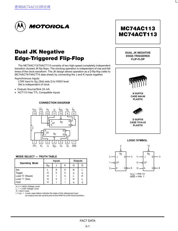
The MC74AC113/74ACT113 consists of two high-speed completely independent transition clocked JK flip-flops. The clocking operation is independent of rise and fall times of the clock waveform. The JK design allows operation as a D flip-flop (refer to MC74AC74/74ACT74 data sheet) by connecting the J and K inputs together. Asynchronous Inputs: LOW input to SD (Set) sets Q to HIGH level Set is independent of clock Outputs Source/Sink 24 m A ′ACT113 Has TTL Compatible Inputs
N SUFFIX CASE 646-06 PLASTIC
CONNECTION DIAGRAM
VCC CP2 K2 J2 SD2 Q2 Q2
D SUFFIX
CASE 751A-03
PLASTIC
LOGIC SYMBOL
CP1 K1 J1 SD1 Q1 Q1 GND
SD SD
MODE SELECT — TRUTH TABLE QJ QJ
Inputs Outputs
Operating Mode CP CP
Set Toggle
VCC = PIN 14
Load “0” (Reset)
GND = PIN 7
Load “1” (Set) Hold H, h = HIGH Voltage Level L, l = LOW Voltage Level X = Don’t Care l, h (q) = Lower case letters indicate the state of the referenced input
(or output) one set-up time prior to the HIGH to LOW clock transition.
FACT DATA 5-1
Page Summary Contents For Motorola MC74AC113 MC74ACT113 Data Sheet
Manual Details
| Brand | Motorola |
|---|---|
| Pages | 6 |
| File Size | 186.47 KB |
| Published | June 05, 2026 |
Enter the captcha to get the download link:

Frequently Asked Questions
How can I operate the device as a D flip-flop?
Connect the J and K inputs together to allow operation as a D flip-flop.
What is the recommended operating temperature range for this device?
The typical extended junction temperature (J T) range is –40 °C to 85 °C, while the storage temperature range is –65 to +150 °C.
What are the electrical specifications for the DC supply voltage and current output?
The recommended V CC DC Supply Voltage is 5.0V (Range: 4.5V to 5.5V). Output currents can sink/source up to ±24 mA.
Does this flip-flop only operate in one mode or multiple modes?
It supports three operating modes: Hold, Toggle, and Set/Load via asynchronous inputs (S for Set, L for Load).