MOTOROLA LF441C LF442C LF444C Data Sheet
Summary
This comprehensive manual provides detailed specifications for LF441C series JFET input operational amplifiers, ideal for low power analog signal conditioning. It covers DC and AC electrical characteristics, maximum ratings, available packages, and technical usage guidelines. Designed for electronics engineers needing reliable, high-precision amplification with features like low bias current and high slew rate in commercial environments.
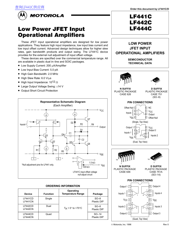
Page 1 Text Content
查询LF441C供应商
Order this document by LF441C/D
These JFET input operational amplifiers are designed for low power
LOW POWER
applications. They feature high input impedance, low input bias current and low input offset current. Advanced design techniques allow for higher slew JFET INPUT rates, gain bandwidth products and output swing. The LF441C device
OPERATIONAL AMPLIFIERS
provides for the external null adjustment of input offset voltage. These devices are specified over the commercial temperature range. All
SEMICONDUCTOR
are available in plastic dual in–line and SOIC packages.
TECHNICAL DATA
Low Supply Current: 200 µA/Amplifier Low Input Bias Current: 5.0 p A High Gain Bandwidth: 2.0 MHz High Slew Rate: 6.0 V/µs High Input Impedance: 1012 Ω Large Output Voltage Swing: ±14 V
N SUFFIX D SUFFIX
Output Short Circuit Protection
PLASTIC PACKAGE PLASTIC PACKAGE CASE 626 CASE 751
(SO–8)
Representative Schematic Diagram PIN CONNECTIONS
(Each Amplifier)
Offset Null NC
Inputs
Output
VEE Offset Null
J1 J2 (Single, Top View)
Inputs R3 R4
Output Output 1 VCC
D1 Output 2
C1 Inputs 1
Q3 +2 Inputs 2
Q1 Q2 (Dual, Top View)
*Null adjustment pins for LF441 only. VEE
100 kΩ N SUFFIX D SUFFIX PLASTIC PACKAGE PLASTIC PACKAGE
LF441C input offset voltage CASE 646 CASE 751A
null adjust circuit (SO–14)
PIN CONNECTIONS
ORDERING INFORMATION Output 1 Output 4
Operating
Temperature Range Inputs 1 Inputs 4
Device Function Package LF441CD Single SO–8
VCC VEE
LF441CN Plastic DIP LF442CD Dual SO–8 Inputs 2 Inputs 3
0° 70°C LF442CN A = to +
Plastic DIP
Output 2 Output 3
LF444CD Quad SO–14 LF444CN Plastic DIP
(Quad, Top View)
Motorola, Inc. 1996 Rev 0
1MOTOROLA ANALOG IC DEVICE DATA
Page Summary Contents For MOTOROLA LF441C LF442C LF444C Data Sheet
Manual Details
| Brand | Motorola |
|---|---|
| Pages | 10 |
| File Size | 211.81 KB |
| Published | May 31, 2026 |
Enter the captcha to get the download link:

Frequently Asked Questions
What are the core electrical specifications for this amplifier?
It boasts a high gain bandwidth of 2.0 MHz, a slew rate of 6.0 V/μs, and an input bias current as low as 5.0 pA.
Does this operational amplifier require calibration after installation?
Yes, the LF441 device provides for external null adjustment of the input offset voltage.
What is the recommended operating temperature range?
These devices are specified and rated for the commercial temperature range of 0° to +70°C.