MOTOROLA 33999 Data Sheet
Summary
The 33999 is a high-performance, 16-output low-side switch designed as a robust bus expander and buffer for microcontroller applications. Utilizing a 24-bit Serial Peripheral Interface (SPI) alongside dedicated PWM controls, it manages complex switching for various loads like relays and LEDs. This advanced component enhances system fault management by isolating the main MCU. The manual provides comprehensive technical specifications for implementing and optimizing its low-voltage control and high-reliability switching capabilities. Ideal for electronics designers building sophisticated embedded systems requiring precise, configurable output control.
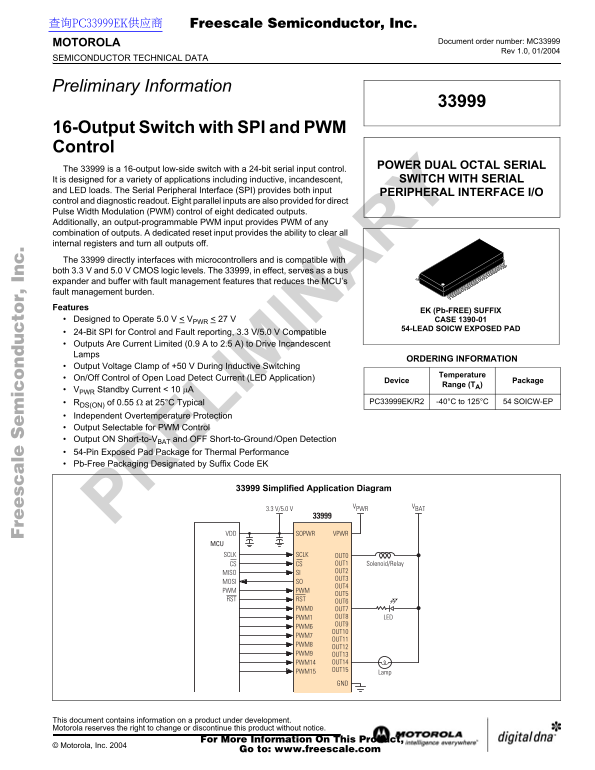
Page 1 Text Content
re sc le ic to r,
查询PC33999EK供应商 Freescale Semiconductor, Inc.
MOTOROLA Document order number: MC33999
Rev 1.0, 01/2004
SEMICONDUCTOR TECHNICAL DATA
Preliminary Information
16-Output Switch with SPI and PWM Control
POWER DUAL OCTAL SERIAL
The 33999 is a 16-output low-side switch with a 24-bit serial input control. It is designed for a variety of applications including inductive, incandescent, SWITCH WITH SERIAL and LED loads. The Serial Peripheral Interface (SPI) provides both input
PERIPHERAL INTERFACE I/O
control and diagnostic readout. Eight parallel inputs are also provided for direct Pulse Width Modulation (PWM) control of eight dedicated outputs. Additionally, an output-programmable PWM input provides PWM of any combination of outputs. A dedicated reset input provides the ability to clear all internal registers and turn all outputs off. The 33999 directly interfaces with microcontrollers and is compatible with both 3.3 V and 5.0 V CMOS logic levels. The 33999, in effect, serves as a bus expander and buffer with fault management features that reduces the MCU’s fault management burden. Features
EK (Pb-FREE) SUFFIX
Designed to Operate 5.0 V < VPWR < 27 V CASE 1390-01
54-LEAD SOICW EXPOSED PAD
24-Bit SPI for Control and Fault reporting, 3.3 V/5.0 V Compatible Outputs Are Current Limited (0.9 A to 2.5 A) to Drive Incandescent Lamps
ORDERING INFORMATION
Output Voltage Clamp of +50 V During Inductive Switching
Temperature
On/Off Control of Open Load Detect Current (LED Application)
Device Package
Range (TA)
VPWR Standby Current < 10 µA
RDS(ON) of 0.55 Ω at 25°C Typical PC33999EK/R2 -40°C to 125°C SOICW-EP
Independent Overtemperature Protection Output Selectable for PWM Control Output ON Short-to-VBAT and OFF Short-to-Ground/Open Detection 54-Pin Exposed Pad Package for Thermal Performance Pb-Free Packaging Designated by Suffix Code EK
33999 Simplified Application Diagram Simplified Application Diagram 33999 Simplified Application Diagram
VPWR VBAT
VDD SOPWR VPWR MCU
SCLKSCLK OUT0
CSCS OUT1 Solenoid/Relay SIMISO OUT2 OUT3
SOMOSI
PWMPWM
RSTRST
PWM0 OUT7
PWM1 OUT8 LED OUT9
OUT10
OUT11
OUT12
PWM9 OUT13
PWM14 OUT14 PWM15 OUT15
This document contains information on a product under development. Motorola reserves the right to change or discontinue this product without notice.
For More Information On This Product,
© Motorola, Inc. 2004
Go to: www.freescale.com
Page Summary Contents For MOTOROLA 33999 Data Sheet
Manual Details
| Brand | Motorola |
|---|---|
| Pages | 16 |
| File Size | 494.39 KB |
| Published | June 02, 2026 |
Enter the captcha to get the download link:

Frequently Asked Questions
What logic levels are compatible with the 33999 device?
It is directly compatible with both 3.3 V and 5.0 V CMOS logic levels.
How does the 33999 manage output faults?
The outputs include protection against overvoltage (clamped at +50 V), open load, short-to-V, and short-to-Gnd detection.
What is the maximum current it can supply to an output?
Each output is current limited between 0.9 A and 2.5 A for driving lamps.
Does the device offer multiple control options for outputs?
Yes, it features a 24-bit SPI interface, eight parallel PWM inputs, and an additional PWM input for controlling any combination of outputs.