# A B C D E F G H I J K L M N O P Q R S T U V W X Y Z

MOTOROLA 33879 Data Sheet

Summary

This professional octal serial switch is an advanced hardware solution for controlling eight power loads—including inductive, incandescent, or LED devices—directly from a microcontroller. Featuring 16-bit SPI control and integrated fault protection, it provides configurable high/low-side switching and supports PWM applications. The accompanying manual details the product's sophisticated electronics, pin functions, circuit schematics, and performance specifications, making it essential for embedded systems engineers developing reliable power management or load-switching equipment.
📄 Preview PAGE OF 21

Page 1 Text Content

re sc le ic to r,

查询PC33879DWB/R2供应商

Freescale Semiconductor, Inc.

MOTOROLA Document order number: MC33879

Rev 3.0, 06/2004

SEMICONDUCTOR TECHNICAL DATA

Preliminary Information

Configurable Octal Serial Switch with Open Load Detect Current

CONFIGURABLE OCTAL SERIAL

Disable

SWITCH WITH OPEN LOAD

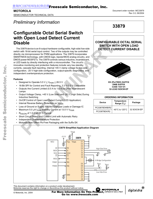
The 33879 device is an 8-output hardware-configurable, high-side/low-side

DETECT CURRENT DISABLE

switch with 16-bit serial input control. Two of the outputs may be controlled directly via microprocessor for PWM applications. The 33879 incorporates SMARTMOS technology, with CMOS logic, bipolar/MOS analog circuitry, and DMOS power MOSFETs. The 33879 controls various inductive, incandescent, or LED loads by directly interfacing with a microcontroller. The circuit’s innovative monitoring and protection features include very low standby currents, cascade fault reporting, internal +45 V clamp voltage for low-side configuration, -20 V high-side configuration, output-specific diagnostics, and independent overtemperature protection.

Features

Designed to Operate 5.5 V < VPWR < 26.5 V EK (Pb-FREE) SUFFIX DWB SUFFIX

16-Bit SPI for Control and Fault Reporting, 3.3 V/5.0 V Compatible

CASE 1437-01

Outputs Are Current Limited (0.5 A to 1.0 A) to Drive Incandescent 32-LEAD SOICW-EP Lamps Output Voltage Clamp, +45 V (Low Side) and -20 V (High Side) During Inductive Switching ORDERING INFORMATION On/Off Control of Open Load Detect Current (LED Application)

Temperature

Device Package

Internal Reverse Battery Protection on VPWR Range (TA) Loss of Ground or Supply Will Not Energize Loads or Damage IC

PC33879DWB/R2

Maximum 5.0 µA IPWR Standby Current at 13.0 V VPWR -40°C to 125°C 32 SOICW-EP

PC33879EK/R2

RDS(ON) of 1.0 Ω at 25°C Typical Short Circuit Detect and Current Limit with Automatic Retry Independent Overtemperature Protection Motorola Now Offers Pb-Free Packaging with the Suffix EK

33879 i Simplified Application Diagram plified Application Diagram VPWR

MCU VDD VPWR D1 D2 D3

A0 EN D4

High-Side Drive

MOSI DI S1 S2

SCLK SCLK

CS CS

MISO DO

H-Bridge Configuration

PWM1 IN5

D5 VBAT

PWM2 IN6 D6 D7 D8

S5 Low-Side Drive

GND S6 S7 S8

This document contains information on a product under development. Motorola reserves the right to change or discontinue this product without notice.

For More Information On This Product,

© Motorola, Inc. 2004

Go to: www.freescale.com

Page Summary Contents For MOTOROLA 33879 Data Sheet

Page 1 re sc le ic to r, 查询PC33879DWB/R2供应商 Freescale Semiconductor, Inc. MOTOROLA Document order number: MC33879 Rev 3.0, 06/2004 SEMICONDUCTOR TECHNICAL DATA Preliminary Information Configurable Octal Seri...
Page 2 re sc le ic to r, Freescale Semiconductor, Inc. VDD VPWR CS Internal Overvoltage Charge Bias Shutdown/POR SCLK Pump Power Supply Sleep State DO GND OV, POR, SLEEP SPI and EN Interface Typical of all 8...
Page 3 re sc le ic to r, Freescale Semiconductor, Inc. GND DO1 VDD VPWR S8 NC NC S7 D8 D7 S2 S4 D2 D4 NC NC NC NC S1 S3 D1 D3 D6 D5 S6 S5 IN6 IN5 EN CS SCLK DI PIN FUNCTION DESCRIPTION Pin Pin Name Formal Na...
Page 4 re sc le ic to r, Freescale Semiconductor, Inc. MAXIMUM RATINGS All voltages are with respect to ground unless otherwise noted. Rating Symbol Value Unit VDD Supply Voltage (Note 1) VDD -0.3 to 7.0 VDC...
Page 5 re sc le ic to r, Freescale Semiconductor, Inc. STATIC ELECTRICAL CHARACTERISTICS Characteristics noted under conditions of 3.1 V ≤ VDD ≤ 5.5 V, 5.5 V ≤ VPWR ≤ 18 V, -40°C ≤ TC ≤ 125°C unless otherwis...
Page 6 re sc le ic to r, Freescale Semiconductor, Inc. STATIC ELECTRICAL CHARACTERISTICS (continued) Characteristics noted under conditions of 3.1 V ≤ VDD ≤ 5.5 V, 5.5 V ≤ VPWR ≤ 18 V, -40°C ≤ TC ≤ 125°C unl...
Page 7 re sc le ic to r, Freescale Semiconductor, Inc. STATIC ELECTRICAL CHARACTERISTICS (continued) Characteristics noted under conditions of 3.1 V ≤ VDD ≤ 5.5 V, 5.5 V ≤ VPWR ≤ 18 V, -40°C ≤ TC ≤ 125°C, un...
Page 8 re sc le ic to r, Freescale Semiconductor, Inc. DYNAMIC ELECTRICAL CHARACTERISTICS Characteristics noted under conditions of 3.1 V ≤ VDD ≤ 5.5 V, 5.5 V ≤ VPWR ≤ 18 V, -40°C ≤ TC ≤ 125°C unless otherwi...
Page 9 re sc le ic to r, Freescale Semiconductor, Inc. DYNAMIC ELECTRICAL CHARACTERISTICS (continued) Characteristics noted under conditions of 3.1 V ≤ VDD ≤ 5.5 V, 5.5 V ≤ VPWR ≤ 18 V, -40°C ≤ TC ≤ 125°C un...
Page 10 re sc le ic to r, Freescale Semiconductor, Inc. Timing Diagrams 0.2 VDD tlead tlag 0.7 VDD 0.2 VDD t DI(su) t DI(hold) 0.7 VDD DI MSB in 0.2 VDD t DO(en) t DO(dis) tvalid DO MSB out LSB out0.7 VDD 0.2...
Page 11 re sc le ic to r, Freescale Semiconductor, Inc. ur re nt in to in (µ ur ur re re nt nt in in to to in in (u (µ ur re nt in to in (m Typical Electrical Characteristics 1.4 VPWR @ 13 VPWR @ 18 High Side...
Page 12 re sc le ic to r, Freescale Semiconductor, Inc. pe Lo ad (µ , O Typical Electrical Characteristics (continued) 5.0 TA = 25°C VPWR @ 16 Open Load Detect Enabled 4.5 TA, Ambient Temperature (°C) TA, Amb...
Page 13 re sc le ic to r, Freescale Semiconductor, Inc. SYSTEM/APPLICATION INFORMATION FUNCTIONAL PIN DESCRIPTION CS Pin follows a first-in, first-out protocol with both input and output words transferring th...
Page 14 re sc le ic to r, Freescale Semiconductor, Inc. MCU INTERFACE DESCRIPTION Introduction Figure 14 illustrates the daisy chain configuration using the 33879. Data from the MCU is clocked daisy chain thr...
Page 15 re sc le ic to r, Freescale Semiconductor, Inc. SPI DEFINITION On each SPI communication, a 16-bit command word is sent 33879 will perform on rising edge of CS. The Fault Register, to the 33879 and a ...
Page 16 re sc le ic to r, Freescale Semiconductor, Inc. DEVICE OPERATION Power Supply SPI Integrity Check The 33879 device has been designed with ultra-low sleep Checking the integrity of the SPI communicatio...
Page 17 re sc le ic to r, Freescale Semiconductor, Inc. An output OFF open load fault is indicated when the drain-to- Output Voltage Clamp source voltage is less than the output threshold voltage Each output ...
Page 18 re sc le ic to r, Freescale Semiconductor, Inc. PACKAGE DIMENSIONS EK (Pb-FREE) SUFFIX DWB SUFFIX 32-LEAD SOIC WIDE BODY EXPOSED PAD PLASTIC PACKAGE CASE 1437-01 ISSUE O PIN 1 ID CL10.9 NOTES: 1. ALL ...
Page 19 re sc le ic to r, Freescale Semiconductor, Inc. NOTES MOTOROLA ANALOG INTEGRATED CIRCUIT DEVICE DATA For More Information On This Product, Go to: www.freescale.com
Page 20 re sc le ic to r, Freescale Semiconductor, Inc. Information in this document is provided solely to enable system and software implementers to use Motorola products. There are no express or implied cop...
Page 21 WWW.ALLDATASHEET.COM Copyright © Each Manufacturing Company. All Datasheets cannot be modified without permission. This datasheet has been download from : www.All Data Sheet.com 100% Free Data Sheet S...

Manual Details

Brand Motorola
Pages 21
File Size 397.52 KB
Published June 02, 2026
52 views

Enter the captcha to get the download link:

captcha

Frequently Asked Questions

How is the MC3379 device primarily controlled?

It uses a 16-bit SPI interface for serial input control, and two outputs can also be controlled directly via PWM using dedicated pins IN5 and IN6.

What is the maximum standby current draw?

The maximum standby current specified for this device is 5.0 µA at 13.0 V.

What types of loads can this module handle?

It controls inductive, incandescent, or LED loads, and features current limiting between 0.5 A to 1.0 A.

What protective functions are built into the circuit?

The device includes independent overtemperature protection, open load detection, and internal clamps (+45 V low side / -20 V high side).