LINEAR TECHNOLOGY LTC6084 LTC6085 Data Sheet Manual
Summary
These low-power, dual/quad CMOS amplifiers are ideal choice for demanding signal processing applications requiring rail-to-rail performance in ultra-low supply voltage environments. Featuring 1pA input bias current, low offset drift, and a stable 1.5MHz bandwidth, they maximize dynamic range while minimizing power usage. The accompanying manual provides detailed technical specifications, various package options (MSOP, DFN), and guides users through integration for applications ranging from data acquisition and medical devices to consumer electronics.
Page 1 Text Content
LTC6084/LTC6085 Dual/Quad 1.5MHz, Rail-to-Rail, CMOS Amplifi ers
FEATURES DESCRIPTION n Low Offset Voltage: 750μV Maximum
The LTC®6084/LTC6085 are dual/quad, low cost, low offset,
n Low Offset Drift: 5μV/°C Maximum
rail-to-rail input/output, unity-gain stable CMOS operational
n Low Input Bias Current:
amplifi ers that feature 1p A of input bias current.
1p A (Typical at 25°C)
A 1.5MHz gain bandwidth, and 0.5V/μs slew rate, along
with the wide supply range and a low 0.75m V offset, make
n Rail-to-Rail Inputs and Outputs
the LTC6084/LTC6085 useful in an extensive variety of ap-
n 2.5V to 5.5V Operation Voltage
plications from data acquisition to medical equipment and
n Gain Bandwidth Product: 1.5MHz
consumer electronics. The 110μA supply current and the
n CMRR: 70d B Minimum
shutdown mode are ideal for signal processing applications
n PSRR: 94d B Minimum
which demand performance with minimal power.
n Supply Current: 110μA per Amplifi er
n Shutdown Current: 1.1μA per Amplifi er The LTC6084/LTC6085 have an output stage which swings n Available in 8-Lead MSOP and 10-Lead DFN within 5m V of either supply rail to maximize signal dynamic
Packages (LTC6084) and 16-Lead SSOP and DFN range in low supply applications. The input common
Packages (LTC6085) IN IA mode range includes the entire supply voltage. These op
amps are specifi ed on power supply voltages of 2.5V and 5V from –40°C to 125°C. The dual amplifi er LTC6084 is
APPLICATIONS
available in 8-lead MSOP and 10-lead DFN packages. The n Portable Test Equipment quad amplifi er LTC6085 is available in 16-lead SSOP and n Medical Equipment DFN packages.
n Consumer Electronics L, LT, LTC and LTM are registered trademarks of Linear Technology Corporation.
All other trademarks are the property of their respective owners.
n Data Acquisition
TYPICAL APPLICATION
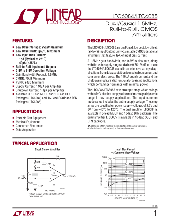
Shock Sensor Amplifi er Input Bias Current
vs Common Mode Voltage
VS = 5V
470p F TA = 125°C 3V
TA = 85°C
LTC6084
100k VOUT = 120m V/g 3V TA = 25°C
60845 TA01 0.1
7Hz TO 5k Hz
*SHOCK SENSOR MURATA ERIE PKGS-OOMX1 0.01 www.murata.com 0.5 2.5 3.5 4.5 541.5
COMMON MODE VOLTAGE (V)
60845 TA01b
60845fa
Page Summary Contents For LINEAR TECHNOLOGY LTC6084 LTC6085 Data Sheet Manual
Manual Details
| Brand | Linear |
|---|---|
| Pages | 16 |
| File Size | 236.60 KB |
| Published | June 16, 2026 |
Enter the captcha to get the download link:

Frequently Asked Questions
What features characterize the LTC6084/LTC6085 amplifiers?
They are low offset voltage (max 750μV), rail-to-rail, unity-gain stable CMOS operational amplifiers with a 1.5MHz gain bandwidth.
Which packages are available for the dual LTC6084 and quad LTC6085 chips?
The LTC6084 is available in 8-Lead MSOP and 10-Lead DFN, while the LTC6085 is available in 16-Lead SSOP and DFN packages.
What is the minimum supply current for a single amplifier when shutdown?
The shutdown current listed for each amplifier is 1.1μA per Amplifier.