# A B C D E F G H I J K L M N O P Q R S T U V W X Y Z

LINEAR TECHNOLOGY LTC4100 User's Manual

Summary

This single-chip smart battery charger controller simplifies complex charging solution design for robust, SBS-compliant systems. The module features highly efficient operation (>98%) and supports essential functions like advanced temperature monitoring via SafetySignal and comprehensive AC adapter current limiting. Designed for use in portable instruments, data storage solutions, and backup servers, it provides precise control over voltage (3.5V to 26V), charging current, and critical parameters, ensuring reliable power management while simplifying system construction.
📄 Preview PAGE OF 28

Page 1 Text Content

LTC4100 Smart Battery

Charger Controller FEATURES DESCRIPTIO

Single Chip Smart Battery Charger Controller The LTC®4100 Smart Battery Charger is a single chip

100% Compliant (Rev. 1.1) SMBus Support Allows charging solution that dramatically simplifies construc- for Operation with or without Host tion of an SBS compliant system. The LTC4100 imple-

SMBus Accelerator Improves SMBus Timing ments a Level 2 charger function whereby the charger can

Wide Output Voltage Range: 3.5V to 26V be programmed by the battery or by the host. A Safety Signal Hardware Interrupt and SMBAlert Response on the battery being charged is monitored for tempera- Eliminate Interrupt Polling ture, connectivity and battery type information. The SMBus High Efficiency Synchronous Buck Charger interface remains alive when the AC power adapter is 0.5V Dropout Voltage; Maximum Duty Cycle > 98% removed and responds to all SMBus activity directed to AC Adapter Current Limit Maximizes Charge Rate it, including Safety Signal status (via the Charger Status ±0.8% Voltage Accuracy; ±4% Current Accuracy command). The charger also provides an interrupt to the Up to 4A Charging Current Capability host whenever a status change is detected (e.g., battery 10-Bit DAC for Charge Current Programming removal, AC adapter connection).

11-Bit DAC for Charger Voltage Programming

Charging current and voltage are restricted to chemistry-

User-Selectable Overvoltage and Overcurrent Limits

specific limits for improved system safety and reliability.

High Noise Immunity Safety Signal Sensor

Limits are programmable by two external resistors. Addi-

Available in a 24-Pin SSOP Package

tionally, the maximum average current from the AC adapter APPLICATIO is programmable to avoid overloading the adapter when simultaneously supplying load current and charging

Portable Instruments and Computers

current. When supplying system load current, charging

Data Storage Systems and Battery Backup Servers

current is automatically reduced to prevent adapter

, LT, LTC and LTM are registered trademarks of Linear Technology Corporation. All

overload.

other trademarks are the property of their respective owners. Protected by U.S. Patents including 6650174 and 5723970.

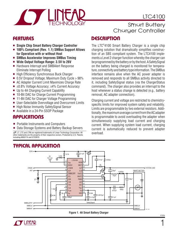
TYPICAL APPLICATIO DCIN

TO 5.5V

LTC4100 0.1µF 0.033Ω

VDD DCIN

DCDIV INFET 5k

CHGEN CHGEN CLP SYSTEM LOAD

ACP ACP CLN 20µF SMART BATTERY

SMBALERT TGATE

SCL BGATE

SDA PGND 20µF

THB CSP THA BAT ILIM VSET

VLIM ITH 0.01µF IDC GND 6.04k10k

SMBALERT# Safety Signal

SMBCLK SMBCLK SMBDAT SMBDAT 4100 TA01

Figure 1. 4A Smart Battery Charger

4100fa

Page Summary Contents For LINEAR TECHNOLOGY LTC4100 User's Manual

Page 1 LTC4100 Smart Battery Charger Controller FEATURES DESCRIPTIO Single Chip Smart Battery Charger Controller The LTC®4100 Smart Battery Charger is a single chip 100% Compliant (Rev. 1.1) SMBus Support Al...
Page 2 LTC4100 ABSOLUTE AXI RATI GS PACKAGE/ORDER I FOR ATIO (Note 1) TOP VIEW ORDER PART Voltage from VDD to GND 7V/–0.3V TGATE CLP NUMBER Voltage from CHGEN, DCDIV, SDA, SCL PGND CLN BGATE BAT and SMBALERT...
Page 3 LTC4100 ELECTRICAL CHARACTERISTICS The ● denotes the specifications which apply over the full operating temperature range, otherwise specifications are at TA = 25°C. VDCIN = 20V, VDD = 3.3V, VBAT = 12...
Page 4 LTC4100 ELECTRICAL CHARACTERISTICS The ● denotes the specifications which apply over the full operating temperature range, otherwise specifications are at TA = 25°C. VDCIN = 20V, VDD = 3.3V, VBAT = 12...
Page 5 LTC4100 ELECTRICAL CHARACTERISTICS The ● denotes the specifications which apply over the full operating temperature range, otherwise specifications are at TA = 25°C. VDCIN = 20V, VDD = 3.3V, VBAT = 12...
Page 6 EF FI CI EN CY LTC4100 TYPICAL PERFOR A CE CHARACTERISTICS INFET Response Time to Reverse Current VOUT vs IOUT PWM Frequency vs Duty Cycle Vgs OF PFET (2V/DIV) Vgs = 0 Vs OF PFET (5V/DIV) OU TP UT OL ...
Page 7 LTC4100 TYPICAL PERFOR A CE CHARACTERISTICS OU TP UT UR RE NT RR OR (A Charging Current Error Charging Voltage Error 0.4 0.150 VDD = 5V VDD = 5V TEMP = 27°C 0.125 TEMP = 27°C 0.3 VLOAD = 12V 0.100 ILO...
Page 8 LTC4100 PI FU CTIO S TGATE (Pin 1): Drives the Top External P-MOSFET of the ACP (Pin 10): This Output Indicates the Value of the DCDIV Battery Charger Buck Converter. Comparator. It can be used to ind...
Page 9 LTC4100 PI FU CTIO S ITH (Pin 19): Control Signal of the Inner Loop of the BAT (Pin 22): Battery Sense Input and the Negative Current Mode PWM. Higher ITH corresponds to higher Reference for the Curre...
Page 10 LTC4100 BLOCK DIAGRA C4 VBAT 100Ω 3k BAT 11-BIT RSENSE VDAC GND 20µF CA1 3k CSP OSCILLATOR CSP WATCHDOG BUFFERED SYSTEM DETECT t ON gm = 1m LOAD 20µF EA CLP +– TGATE ICMP CSP Q2 PWM IREV LOGIC D1 BGAT...
Page 11 LTC4100 TEST CIRCUIT LTC4100 BAT VDAC VDAC FOR VDAC CSP BAT VSET ITH CLN CLP LT1055 4100 TC01 4100fa
Page 12 LTC4100 OPERATIO Overview (Refer to Block Diagram) comparator IREV, or the beginning of the next cycle. The oscillator uses the equation, The LTC4100 is composed of a battery charger section, a charge...
Page 13 LTC4100 OPERATIO PWM Watchdog Timer Description of Supported Battery Charger Functions There is a watchdog timer that observes the activity on the The functions are described as follows (see Table 1 a...
Page 14 LTC4100 OPERATIO Table 1: Summary of Supported Charger Functions SMBus Command Data Function Access Address Code Type D15 D14 D13 D12 D11 D10 D9 D8 D7 D6 D5 D4 D3 D2 D1 DO Charger Spec Info() 7'b0001_...
Page 15 LTC4100 OPERATIO The ENABLE_POLLING bit is not supported by the LTC4100. The RES_COLD bit is set only when the Safety Signal Values written to this bit are ignored. resistance value is greater than 28...
Page 16 LTC4100 OPERATIO AC_PRESENT will activate the LTC4100 SMBALERT pull- Input: The CHARGING_VOLTAGE is an unsigned 16-bit down. integer specifying the requested charging voltage in m V. The LTC4100 consi...
Page 17 LTC4100 OPERATIO Purpose: This function allows the SMBus Host to deter- Change of BATTERY_PRESENT in the Charger Status() mine if the battery charger is an LTC4100. Identifying the function. manufactu...
Page 18 LTC4100 OPERATIO 3. The host may control charging by disabling the Smart 9. There is insufficient DCIN voltage to charge the battery. Battery’s ability to transmit Charging Current() and The LTC4100 w...
Page 19 LTC4100 OPERATIO ues, when there is sufficient DCIN voltage to charge the range is determined, the lower value thresholds are not battery. sampled. The Safety Signal decoder block uses the previ- ousl...
Page 20 LTC4100 OPERATIO Table 4. Safety Signal State Ranges Table 6. ILIM Trip Points and Ranges Safety Signal CHARGE EXTERNAL CONTROLLED RESISTANCE STATUS BITS DESCRIPTION RESISTOR CHARGING (RILIM) ILIM VOL...
Page 21 LTC4100 OPERATIO CH AR GE UT (V IPROG RVLIM = 33k (FROM CA1 AMP) ∆-∑ CHARGING_CURRENT MODULATOR VALUE Figure 7. Current DAC Operation PROGRAMMED VALUE (V) AVERAGE CHARGER CURRENT ILIMIT/8 NOTE: THE LT...
Page 22 LTC4100 APPLICATIO S I FOR ATIO Adapter Limiting RCL = 100m V/ILIM ILIM = Adapter Min Current – An important feature of the LTC4100 is the ability to (Adapter Min Current • 7%) automatically adjust ch...
Page 23 LTC4100 APPLICATIO S I FOR ATIO Table 9. Recommended Resistor Values Table 10. Recommended Inductor Values IMAX (A) RSENSE (Ω) 1% RSENSE (W) RILIM (Ω) 1% Maximum Input Minimum Inductor Average Current...
Page 24 LTC4100 APPLICATIO S I FOR ATIO Where δ∆T is the temperature dependency of RDS(ON) and MOSFET. Use 6V for the gate voltage swing and VDCIN for k is a constant inversely related to the gate drive curre...
Page 25 LTC4100 APPLICATIO S I FOR ATIO Input and Output Capacitors tween the battery and the output capacitor depending on the ESR of the output capacitor and the battery imped- In the 4A Lithium Battery Cha...
Page 26 LTC4100 APPLICATIO S I FOR ATIO list for proper layout. Layout the PCB using this specific as a single pair on the same layer at any given time with order. smallest trace spacing possible. Locate any ...
Page 27 LTC4100 PACKAGE DESCRIPTIO G Package 24-Lead Plastic SSOP (5.3mm) (Reference LTC DWG # 05-08-1640) 0.42 ±0.03 0.65 BSC RECOMMENDED SOLDER PAD LAYOUT BSC 0.05 NOTE: (.002) 1. CONTROLLING DIMENSION: MIL...
Page 28 LTC4100 TYPICAL APPLICATIO LTC4100 Li-Ion Battery Charger ILIM = 4A/VLIM = 17.4V, Adapter Rating = 2.7A RCL 0.033Ω 15V TO 20V SYSTEM C9 LOAD FROM WALL C1 R1 ADAPTER 0.1µF 4.9k 10V DCIN D6 INFET CLNCLP...

Manual Details

Brand Linear
Pages 28
File Size 285.41 KB
Published June 19, 2026
2 views

Enter the captcha to get the download link:

captcha

Frequently Asked Questions

What are the key features of the LTC4100 charger controller?

It is a single chip that offers SMBus compliance, high efficiency synchronous buck charging with up to 4A capability, and programmable limits for safety.

How can I program the optimal charging status or limitations?

You can program charge current and voltage using 11-Bit and 10-Bit DACs respectively. Furthermore, Overvoltage/Overcurrent Limits are user-selectable via external resistors.

Does the charger system automatically manage power when supplying a load?

Yes, it automatically reduces charging current to prevent the AC adapter from overloading when simultaneously supplying load current.