# A B C D E F G H I J K L M N O P Q R S T U V W X Y Z

LINEAR TECHNOLOGY LTC3727 LTC3727-1 User's Manual

Summary

This high-performance, dual 2-phase synchronous step-down switcher regulator is essential for powering demanding digital electronics and battery systems. It delivers exceptional efficiency across a wide output voltage range, utilizing out-of-phase control techniques to minimize power loss and noise. Engineered with features like low dropout operation, soft-start, and robust protection schemes, it ensures stable power delivery even during transient load changes. The manual provides comprehensive technical specifications, advanced operational guidance, and application details for engineers designing reliable telecom or battery-powered equipment.
📄 Preview PAGE OF 32

Page 1 Text Content

LTC3727/LTC3727-1 High Efficiency, 2-Phase

Synchronous Step-Down Switching Regulators

FEATURES DESCRIPTIO Wide Output Voltage Range: 0.8V ≤ VOUT ≤ 14V The LTC®3727/LTC3727-1 are high performance dual Out-of-Phase Controllers Reduce Required Input step-down switching regulator controllers that drive all Capacitance and Power Supply Induced Noise N-channel synchronous power MOSFET stages. A con-

OPTI-LOOP® Compensation Minimizes COUT stant frequency current mode architecture allows phase-

±1% Output Voltage Accuracy lockable frequency of up to 550k Hz. Power loss and noise

Power Good Output Voltage Monitor due to the ESR of the input capacitors are minimized by Phase-Lockable Fixed Frequency 250k Hz to 550k Hz operating the two controller output stages out of phase.

Latched Short-Circuit Shutdown (LTC3727 Only)

OPTI-LOOP compensation allows the transient response

Dual N-Channel MOSFET Synchronous Drive

to be optimized over a wide range of output capacitance and

Wide VIN Range: 4V to 36V Operation

ESR values. There is a precision 0.8V reference and a power

Very Low Dropout Operation: 99% Duty Cycle

good output indicator. A wide 4V to 30V (36V maximum)

Adjustable Soft-Start Current Ramping

input supply range encompasses all battery chemistries.

Foldback Output Current Limiting

Output Overvoltage Protection A RUN/SS pin for each controller provides soft-start, and Low Shutdown IQ: 20µA on the LTC3727GN, optional timed, short-circuit shut- Selectable Constant Frequency or Burst Mode® down. Current foldback limits MOSFET heat dissipation Operation during short-circuit conditions when overcurrent latchoff Small 28-Lead SSOP Package is disabled. Output overvoltage protection circuitry latches LTC3727-1 Also Available in the 5mm × 5mm QFN on the bottom MOSFET until VOUT returns to normal. The Package FCB mode pin can select among Burst Mode, constant frequency mode and continuous inductor current mode or

APPLICATIO S regulate a secondary winding.

, LTC and LT are registered trademarks of Linear Technology Corporation. Burst Mode

Telecom Systems

and OPTI-LOOP are registered trademarks of Linear Technology Corporation. All other Automotive Systems trademarks are the property of their respective owners. Protected by U.S. Patents, including 5481178, 5929620, 6177787, 6144194, 6100678, 5408150, 6580258, 6304066, 5705919.

Battery-Operated Digital Devices

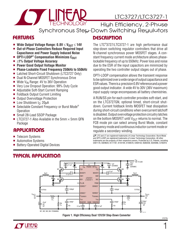
TYPICAL APPLICATIO

VIN 18V TO 28V 22µF

CERAMIC

VIN PGOOD INTVCC CERAMIC

M1 TG1 TG2 M3

8µH BOOST1 BOOST2 15µH

SW1 SW2 LTC3727/

M2 BG1 LTC3727-1 BG2 M4

PLLIN PGND

SENSE1+ SENSE2+

SENSE1– SENSE2–

VOUT1 VOUT2

5V VOSENSE1 VOSENSE2 12V

1% ITH1 ITH2

47µF 220p F RUN/SS1 SGND RUN/SS2 220p F 20k

1% 15k 15k SP

SP 0.1µF 0.1µF

M1, M2, M3, M4: FDS6680A

Figure 1. High Efficiency Dual 12V/5V Step-Down Converter

3727fb

Page Summary Contents For LINEAR TECHNOLOGY LTC3727 LTC3727-1 User's Manual

Page 1 LTC3727/LTC3727-1 High Efficiency, 2-Phase Synchronous Step-Down Switching Regulators FEATURES DESCRIPTIO Wide Output Voltage Range: 0.8V ≤ VOUT ≤ 14V The LTC®3727/LTC3727-1 are high performance dual ...
Page 2 LTC3727/LTC3727-1 ABSOLUTE AXI U RATI GS (Note 1) Input Supply Voltage (VIN) .........................36V to –0.3V ITH1, ITH2, VOSENSE1, VOSENSE2 Voltages ...2.7V to –0.3V Top Side Driver Voltages Pea...
Page 3 LTC3727/LTC3727-1 ELECTRICAL CHARACTERISTICS The ● denotes the specifications which apply over the full operating temperature range, otherwise specifications are at TA = 25°C. VIN = 15V, VRUN/SS1, 2 =...
Page 4 EF FI CI EN CY LTC3727/LTC3727-1 ELECTRICAL CHARACTERISTICS The ● denotes the specifications which apply over the full operating temperature range, otherwise specifications are at TA = 25°C. VIN = 15V...
Page 5 (m V) (m V) SU PP LY UR RE NT (µ A) EN SE EN SE LTC3727/LTC3727-1 TYPICAL PERFOR A CE CHARACTERISTICS Supply Current vs Input Voltage and Mode (Figure 13) EXTVCC Voltage Drop Internal 7.5V LDO Line Re...
Page 6 EN SE (µ A) LTC3727/LTC3727-1 TYPICAL PERFOR A CE CHARACTERISTICS Dropout Voltage vs Output Current SENSE Pins Total Source Current (Figure 13) RUN/SS Current vs Temperature 1.4 1.8 VOUT = 5V RSENSE =...
Page 7 CU RR EN SE NS IN PU CU RR EN (µ A) LTC3727/LTC3727-1 TYPICAL PERFOR A CE CHARACTERISTICS UN DE RV OL TA GE OC KO UT (V Current Sense Pin Input Current EXTVCC Switch Resistance Oscillator Frequency vs...
Page 8 LTC3727/LTC3727-1 PI FU CTIO S PLLFLTR (Pin 5/Pin 2): The phase-locked loop’s lowpass EXTVCC (Pin 22/Pin 21): External Power Input to an filter is tied to this pin. Alternatively, this pin can be driv...
Page 9 LTC3727/LTC3727-1 FU CTIO AL DIAGRA PLLIN INTVCC VIN FIN PHASE DET DUPLICATE FOR SECOND DB 50k BOOST CONTROLLER CHANNEL PLLFLTR TG CB RLP OUT CIND1 OSCILLATOR CLK2 DET BOT FCB 0.86V TOP ON SWITCH INTV...
Page 10 LTC3727/LTC3727-1 OPERATIO (Refer to Functional Diagram) The top MOSFET drivers are biased from floating boot- having the hysteretic comparator follow the error ampli- strap capacitor CB, which normal...
Page 11 LTC3727/LTC3727-1 (Refer to Functional Diagram)OPERATIO Power Good (PGOOD) Pin THEORY AND BENEFITS OF 2-PHASE OPERATION The PGOOD pin is connected to an open drain of an internal The LTC3727 dual high...
Page 12 LTC3727/LTC3727-1 (Refer to Functional Diagram)OPERATIO 5V SWITCH 20V/DIV 3.3V SWITCH 20V/DIV INPUT CURRENT 5A/DIV INPUT VOLTAGE 500m V/DIV 3727 F03a IIN(MEAS) = 1.55ARMS 3727 F03b IIN(MEAS) = 2.53ARM...
Page 13 LTC3727/LTC3727-1 APPLICATIO S I FOR ATIO Figure 1 on the first page is a basic LTC3727/LTC3727-1 application circuit. External component selection is driven by the load requirement, and begins with t...
Page 14 LTC3727/LTC3727-1 APPLICATIO S I FOR ATIO The inductor value also has secondary effects. The transi- The peak-to-peak drive levels are set by the INTVCC tion to Burst Mode operation begins when the av...
Page 15 LTC3727/LTC3727-1 APPLICATIO S I FOR ATIO short-circuit when the synchronous switch is on close to the capacitor is important for capacitor power dissipation 100% of the period. as well as overall bat...
Page 16 LTC3727/LTC3727-1 APPLICATIO S I FOR ATIO The benefit of the LTC3727 multiphase can be calculated discharging term but can be compensated for by using by using the equation above for the higher power ...
Page 17 LTC3727/LTC3727-1 APPLICATIO S I FOR ATIO INTVCC Regulator EXTVCC Connection An internal P-channel low dropout regulator produces The LTC3727 contains an internal P-channel MOSFET 7.5V at the INTVCC p...
Page 18 LTC3727/LTC3727-1 APPLICATIO S I FOR ATIO VIN Output Voltage OPTIONAL EXTVCC CONNECTION The LTC3727 output voltages are each set by an external 7.5V < VSEC < 8.5V feedback resistive divider care...
Page 19 LTC3727/LTC3727-1 APPLICATIO S I FOR ATIO VIN INTVCC Regulating an output voltage of 1.8V, the maximum value 3.3V OR 5V RUN/SS of R1 should be 32K. Note that for an output voltage above RSS* RSS* 2.4V...
Page 20 LTC3727/LTC3727-1 APPLICATIO S I FOR ATIO Why should you defeat overcurrent latchoff? During the The resulting short-circuit current is: prototyping stage of a design, there may be a problem with nois...
Page 21 LTC3727/LTC3727-1 APPLICATIO S I FOR ATIO The phase detector used is an edge sensitive digital type Minimum On-Time Considerations which provides zero degrees phase shift between the Minimum on-time t...
Page 22 LTC3727/LTC3727-1 APPLICATIO S I FOR ATIO be drawn from the inductor primary in order to extract loading conditions. The open-loop DC gain of the control power from the auxiliary windings. With the lo...
Page 23 LTC3727/LTC3727-1 APPLICATIO S I FOR ATIO which excludes MOSFET driver and control currents; the 4. Transition losses apply only to the topside MOSFET(s), second is the current drawn from the 3.3V lin...
Page 24 LTC3727/LTC3727-1 APPLICATIO S I FOR ATIO overshoot seen at this pin. The bandwidth can also be approximately 25 • CLOAD. Thus a 10µF capacitor would estimated by examining the rise time at the pin. T...
Page 25 LTC3727/LTC3727-1 APPLICATIO S I FOR ATIO Design Example A short-circuit to ground will result in a folded back current As a design example for one channel, assume VIN = 24V(nominal), VIN = 30V(max), ...
Page 26 LTC3727/LTC3727-1 APPLICATIO S I FOR ATIO 2. Are the signal and power grounds kept separate? The along the high current input feeds from the input combined LTC3727 signal ground pin and the ground cap...
Page 27 LTC3727/LTC3727-1 APPLICATIO S I FOR ATIO L1SW1 RSENSE1 VOUT1 COUT1 RL1D1 RIN CIN L2SW2 RSENSE2 VOUT2 COUT2 RL2D2BOLD LINES INDICATE HIGH SWITCHING CURRENT. KEEP LINES TO A MINIMUM LENGTH Figure 11. B...
Page 28 LTC3727/LTC3727-1 APPLICATIO S I FOR ATIO application. The frequency of operation should be main- Investigate whether any problems exist only at higher tained over the input voltage range down to drop...
Page 29 LTC3727/LTC3727-1 TYPICAL APPLICATIO S VPULL-UP (<7V) RUN/SS1 PGOOD PGOOD L1 8µH 0.1µF 0.015Ω VOUT1 SENSE1+ TG1 5V 27p F 1000p F 5A; 6A PEAK 1% SENSE1– SW1 VOSENSE1 BOOST1 0.01µF PLLFLTR VIN COUT1 ...
Page 30 LTC3727/LTC3727-1 TYPICAL APPLICATIO S VPULL-UP (<7V) RUN/SS1 PGOOD PGOOD L1 8µH 0.1µF 0.015Ω VOUT1 SENSE1+ TG1 5V 27p F 1000p F 5A; 6A PEAK 1% SENSE1– SW1 VOSENSE1 BOOST1 PLLFLTR VIN COUT1 PLLIN B...
Page 31 LTC3727/LTC3727-1 PACKAGE DESCRIPTIO G Package 28-Lead Plastic SSOP (5.3mm) (Reference LTC DWG # 05-08-1640) 5.00 – 5.60** 0.42 ±0.03 0.65 BSC RECOMMENDED SOLDER PAD LAYOUT MAX BSC 0.05 NOTE: (.002) (...
Page 32 LTC3727/LTC3727-1 RELATED PARTS PART NUMBER DESCRIPTION COMMENTS TM Current Mode Synchronous Step-Down Controllers LTC1625/LTC1775 No RSENSE 97% Efficiency, No Sense Resistor, 16-Pin SSOP LTC1702 No R...

Manual Details

Brand Linear
Pages 32
File Size 428.42 KB
Published June 16, 2026
5 views

Enter the captcha to get the download link:

captcha

Frequently Asked Questions

What is the minimum operating voltage range for this controller?

The Wide V Range allows operation from 4V to 36V (36V maximum).

How can I minimize power loss due to input capacitor ESR?

The device uses an OPTI-LOOP compensation routine which minimizes power loss and noise caused by the ESR of input capacitors.

Does this device protect against overcurrent and short circuits?

Yes. It features Foldback Output Current Limiting and provides Latched Short-Circuit Shutdown (on LTC3727 only).

Is fine-tuning or soft start possible?

Yes. A RUN/SS pin is available for each controller to provide adjustable soft-start current ramping.