# A B C D E F G H I J K L M N O P Q R S T U V W X Y Z

LINEAR TECHNOLOGY LTC2440 Product Specifications User Manual (1), (1)

Summary

This high speed, 24-bit Differential Delta-Sigma ADC provides precise data acquisition with exceptional accuracy and no conversion latency. It features selectable resolutions/speeds, outstanding noise rejection (50/60Hz), and ultra-low power consumption suitable for battery-operated devices. This manual details the extensive electrical characteristics, technical specifications, serial interface programming, and advanced features—including automatic ranging and low-power sleep modes—making it ideal for professionals developing sensitive measurement systems like weight scales or high-speed data acquisition equipment.
📄 Preview PAGE OF 28

Page 1 Text Content

LTC2440

24-Bit High Speed Differential Δ∑ ADC with

Selectable Speed/Resolution

FEATURES DESCRIPTION n Up to 3.5k Hz Output Rate

The LTC®2440 is a high speed 24-bit No Latency Δ∑TM

n Selectable Speed/Resolution

ADC with 5ppm INL and 5μV offset. It uses proprietary

n 2μVRMS Noise at 880Hz Output Rate

delta-sigma architecture enabling variable speed and reso-

n 200n VRMS Noise at 6.9Hz Output Rate with

lution with no latency. Ten speed/resolution combinations

Simultaneous 50/60Hz Rejection (6.9Hz/200n VRMS to 3.5k Hz/25μVRMS) are programmed n 0.0005% INL, No Missing Codes

through a simple serial interface. Alternatively, by tying a

n Autosleep Enables 20μA Operation at 6.9Hz

single pin HIGH or LOW, a fast (880Hz/2μVRMS) or ultralow

n <5μV Offset (4.5V < VCC < 5.5V, –40°C to 85°C)

noise (6.9Hz, 200n VRMS, 50/60Hz rejection) speed/reso-

n Differential Input and Differential Reference with

lution combination can be easily selected. The accuracy

GND to VCC Common Mode Range (offset, full-scale, linearity, drift) and power dissipation n No Latency, Each Conversion is Accurate Even After

are independent of the speed selected. Since there is no

an Input Step latency, a speed/resolution change may be made between n Internal Oscillator—No External Components

conversions with no degradation in performance.

n Pin Compatible with the LTC2410

Following each conversion cycle, the LTC2440 automati-

n 24-Bit ADC in Narrow 16-Lead SSOP Package

cally enters a low power sleep state. Power dissipation may be reduced by increasing the duration of this sleep APPLICATIONS state. For example, running at the 3.5k Hz conversion speed but reading data at a 100Hz rate draws 240μA average

n High Speed Multiplexing

current (1.1m W) while reading data at a 7Hz output rate

n Weight Scales

draws only 25μA (125μW).The LTC2440 communicates

n Auto Ranging 6-Digit DVMs

through a fl exible 3-wire or 4-wire digital interface that is

n Direct Temperature Measurement

compatible with the LTC2410 and is available in a narrow

n High Speed Data Acquisition

16-lead SSOP package. , LT, LTC and LTM are registered trademarks of Linear Technology Corporation. No Latency Δ∑ is a trademark of Linear Technology Corporation. All other trademarks are the property of their respective owners.

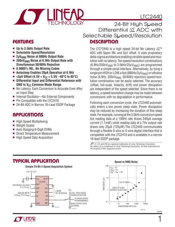
TYPICAL APPLICATION Speed vs RMS Noise Simple 24-Bit 2-Speed Acquisition System

VCC = 5V VREF = 5V 4.5V TO 5.5V + = VIN – = 0V VIN

VCC BUSY LTC2440 2μV AT 880Hz

f OREF+

REFERENCE VOLTAGE

0.1V TO VCC 200n V AT 6.9Hz

REF– SCK

VCC (50/60Hz REJECTION)

3-WIRE

IN+ SDO

ANALOG INPUT SPI INTERFACE 6.9Hz, 200n V NOISE, –0.5VREF TO 0.5VREF 50/60Hz REJECTION

IN– CS

10-SPEED SERIAL

PROGRAMMABLE

GND EXT 880Hz OUTPUT RATE,

2μV NOISE CONVERSION RATE (Hz)

2440 TA01

2440 TA01

2440 TA02

2440fc

Page Summary Contents For LINEAR TECHNOLOGY LTC2440 Product Specifications User Manual (1), (1)

Page 1 LTC2440 24-Bit High Speed Differential Δ∑ ADC with Selectable Speed/Resolution FEATURES DESCRIPTION n Up to 3.5k Hz Output Rate The LTC®2440 is a high speed 24-bit No Latency Δ∑TM n Selectable Speed/R...
Page 2 LTC2440 PIN CONFIGURATION ABSOLUTE MAXIMUM RATINGS (Notes 1,2) Supply Voltage (VCC) to GND ....................... –0.3V to 6V TOP VIEW Analog Input Pins Voltage GND to GND ..............................
Page 3 LTC2440 ANALOG INPUT AND REFERENCE The l denotes the specifi cations which apply over the full operating temperature range, otherwise specifi cations are at TA = 25°C. (Note 3) SYMBOL PARAMETER CONDIT...
Page 4 LTC2440 POWER REQUIREMENTS The l denotes the specifi cations which apply over the full operating temperature range, otherwise specifi cations are at TA = 25°C. (Note 3) SYMBOL PARAMETER CONDITIONS MIN...
Page 5 IN F) IN F) IN LTC2440 TYPICAL PERFORMANCE CHARACTERISTICS Integral Nonlinearity Integral Nonlinearity f OUT = 3.5k Hz f OUT = 1.76k Hz Integral Nonlinearity f OUT = 880Hz VCC = 5V VINCM = 2.5V VCC = ...
Page 6 FU -S IN F) IN LTC2440 TYPICAL PERFORMANCE CHARACTERISTICS Integral Nonlinearity Integral Nonlinearity f OUT = 6.875Hz vs Conversion Rate Integral Nonlinearity vs VINCM VCC = 5V VINCM = 2.5V VCC = 5V ...
Page 7 FF FF FU -S F) LTC2440 TYPICAL PERFORMANCE CHARACTERISTICS Negative Full-Scale Error Positive Full-Scale Error vs Temperature vs Temperature Offset Error vs VCC VCC = 4.5V VCC = 5.5V, 5V VREF = 2.5V O...
Page 8 LTC2440 PIN FUNCTIONS GND (Pins 1, 8, 9, 16): Ground. Multiple ground pins is selected. The device generates its own SCK signal and internally connected for optimum ground current fl ow and outputs th...
Page 9 LTC2440 FUNCTIONAL BLOCK DIAGRAM INTERNAL OSCILLATOR GND AUTOCALIBRATION AND CONTROL (INT/EXT) IN+ IN– ADC SCK SERIAL DECIMATING FIR INTERFACE REF+ REF– Figure 1. Functional Block Diagram TEST CIRCUIT...
Page 10 LTC2440 APPLICATIONS INFORMATION Initially, the LTC2440 performs a conversion. Once the Power-Up Sequence conversion is complete, the device enters the sleep state. The LTC2440 automatically enters an...
Page 11 LTC2440 APPLICATIONS INFORMATION 0.5 • VREF where VREF = REF+ – REF–. Outside this range, indicator (SIG). If VIN is &gt;0, this bit is HIGH. If VIN is &lt;0, the converter indicates the overrange or ...
Page 12 LTC2440 APPLICATIONS INFORMATION microcontroller. Bit 31 (EOC) can be captured on the fi rst Serial Clock Input/Output (SCK) rising edge of SCK. Bit 30 is shifted out of the device on The serial clock...
Page 13 LTC2440 APPLICATIONS INFORMATION Chip Select Input (CS) Serial Data Input (SDI)—Serial Input Speed Selection The active LOW chip select, CS (Pin 11), is used to test the SDI may also be programmed by ...
Page 14 LTC2440 APPLICATIONS INFORMATION CS SDI OSR4* OSR3 OSR2 OSR1 OSR0 BIT 31 BIT 30 BIT 29 BIT 28 BIT 27 BIT 26 BIT 25 BIT 1 BIT 0 Hi-Z Hi-Z SDO EOC “0” SIG MSB LSB *OSR4 BIT MUST BE AT FIRST SCK RISING E...
Page 15 LTC2440 APPLICATIONS INFORMATION 4.5V TO 5.5V VCC BUSY LTC2440 = EXTERNAL OSCILLATOR REF+ f O REFERENCE VOLTAGE = INTERNAL OSCILLATOR 0.1V TO VCC SCK 3-WIRE IN+ SDO ANALOG INPUT RANGE SPI INTERFACE –0...
Page 16 LTC2440 APPLICATIONS INFORMATION 4.5V TO 5.5V VCC BUSY LTC2440 = EXTERNAL OSCILLATOR f OREF+ REFERENCE VOLTAGE = INTERNAL OSCILLATOR 0.1V TO VCC SCK 3-WIRE IN+ SDO ANALOG INPUT RANGE SPI INTERFACE –0....
Page 17 LTC2440 APPLICATIONS INFORMATION controller indicating the conversion result is ready. EOC Once CS is pulled LOW, SCK goes LOW and EOC is output = 1 (BUSY = 1) while the conversion is in progress and ...
Page 18 LTC2440 APPLICATIONS INFORMATION on this fi rst rising edge of SCK and concludes after the new conversion. This is useful for systems not requiring 32nd rising edge. Data is shifted out the SDO pin on...
Page 19 LTC2440 APPLICATIONS INFORMATION 4.5V TO 5.5V VCC BUSY LTC2440 = EXTERNAL OSCILLATOR f OREF+ REFERENCE VOLTAGE = INTERNAL OSCILLATOR 0.1V TO VCC SCK REF– 2-WIRE SPI INTERFACE IN+ SDO ANALOG INPUT RANG...
Page 20 LTC2440 APPLICATIONS INFORMATION JE IO Table 5. OSR vs Notch Frequency (f N) with Internal Oscillator OSR, the noise performance of the device is 200n VRMS with Running at 9MHz better than 80d B rejec...
Page 21 LTC2440 APPLICATIONS INFORMATION The sample rate f S and NULL f N, my also be adjusted by Reduced Power Operation driving the f O pin with an external oscillator. The sample In addition to adjusting t...
Page 22 LTC2440 APPLICATIONS INFORMATION CONVERTER SLEEP CONVERT SLEEP CONVERT SLEEP STATE DATA DATA OUT OUT SUPPLY CURRENT Figure 15. Reduced Power Timing Mode LTC2440 Input Structure When using the internal...
Page 23 LTC2440 APPLICATIONS INFORMATION Direct Connection to Low Impedance Sources Buffering the LTC2440 If the ADC can be located physically close to the sensor, Many applications will require buffering, pa...
Page 24 LTC2440 APPLICATIONS INFORMATION /D IV fastest expected input signal. Figure 20 shows the large For more information on testing high linearity ADCs, refer signal response of the circuit in Figure 19. ...
Page 25 LTC2440 APPLICATIONS INFORMATION Table 6 lists the properties of the LTC2440 with various the modulator sample rate of 1.8MHz) exceeds 120d B. combinations of oversample ratio and clock frequency. Thi...
Page 26 LTC2440 APPLICATIONS INFORMATION Example: The total noise is the RMS sum of this noise with the 200n V noise of the ADC at OSR = 32768. If an amplifi er (e.g. LT1219) driving the input of an LTC2440 h...
Page 27 LTC2440 PACKAGE DESCRIPTION GN Package 16-Lead Plastic SSOP (Narrow .150 Inch) (Reference LTC DWG # 05-08-1641) .009 (0.229) REF .254 MIN .150 – .165 .0015 .0250 BSC.0165 ± RECOMMENDED SOLDER PAD LAYO...
Page 28 LTC2440 TYPICAL APPLICATION VREF 100k +7V VREF TOP_P 5,6,7,8 LT1461-5 TOP_N 100k 2X LT1677 100Ω 0.1% LTC2440 0.047μF REF– BOTTOM_P 2X SILICONIX SI9801 BOTTOM_N Figure 23. Bridge Reversal Eliminates 1/...

Manual Details

Brand Linear
Pages 28
File Size 312.26 KB
Published May 31, 2026
72 views

Enter the captcha to get the download link:

captcha

Frequently Asked Questions

What is the LTC2440's key feature regarding data accuracy and speed?

It offers a No Latency, differential delta-sigma architecture, meaning each conversion is accurate even after speed or resolution changes.

Does the device have low-power modes for energy saving?

Yes, it automatically enters a low power sleep state after each conversion cycle. Power consumption can be reduced by increasing the duration of this sleep state.

What operating temperature range does the LTC2440 support?

The standard package (LTC2440C) operates from 0°C to 70°C, while the 'I' version (LTC2440I) supports –40°C to 85°C.

How does the LTC2440 interface with other components?

It uses a simple serial interface and features an SPI interface for programmability. It is also pin compatible with the LTC2410.