# A B C D E F G H I J K L M N O P Q R S T U V W X Y Z

LINEAR TECHNOLOGY LT1934 LT1934-1 User's Manual

Summary

Optimize your power management solutions with this micropower step-down DC/DC converter. Ideal for engineers designing battery-powered or complex electronic systems, the LT1934 provides efficient voltage regulation across a wide input range (3.2V to 34V). The manual offers comprehensive coverage, detailing low quiescent current performance, high efficiency in various modes, and numerous applications ranging from automotive batteries to industrial controls. Learn about package options, precise technical specifications, and optimal circuit integration for reliable power delivery.
📄 Preview PAGE OF 20

Page 1 Text Content

LT1934/LT1934-1

Micropower Step-Down Switching Regulators in Thin SOT and DFN

FEATURES DESCRIPTION n Wide Input Voltage Range: 3.2V to 34V

The LT®1934 is a micropower step-down DC/DC converter

n Micropower Operation: IQ = 12μA

with internal 400m A power switch, packaged in a low

n 5V at 250m A from 6.5V to 34V Input (LT1934) profi le (1mm) Thin SOT. With its wide input range of 3.2V n 5V at 60m A from 6.5V to 34V Input (LT1934-1) to 34V, the LT1934 can regulate a wide variety of power n 3.3V at 250m A from 4.5V to 34V Input (LT1934) sources, from 4-cell alkaline batteries and 5V logic rails n 3.3V at 60m A from 4.5V to 34V Input (LT1934-1) to unregulated wall transformers and lead-acid batteries. n Low Shutdown Current: <1μA Quiescent current is just 12μA and a zero current shut- n Low VCESAT Switch: 200m V at 300m A down mode disconnects the load from the input source, n Low Profi le (1mm) SOT-23 (Thin SOTTM) and simplifying power management in battery-powered sys-

(2mm × 3mm × 0.8mm) 6-Pin DFN Package tems. Burst Mode® operation and the low drop internal power switch result in high effi ciency over a broad range of load current.

APPLICATIONS

The LT1934 provides up to 300m A of output current. The

FF IC IE

n Wall Transformer Regulation LT1934-1 has a lower current limit, allowing optimum n Automotive Battery Regulation choice of external components when the required output n Standby Power for Portable Products current is less than 60m A. Fast current limiting protects n Distributed Supply Regulation the LT1934 and external components against shorted n Industrial Control Supplies outputs, even at 34V input.

, LT, LTC and LTM are registered trademarks of Linear Technology Corporation. Burst Mode is a registered trademark of Linear Technology Corporation. Thin SOT is a trademark of Linear Technology Corporation. All other trademarks are the property of their respective owners.

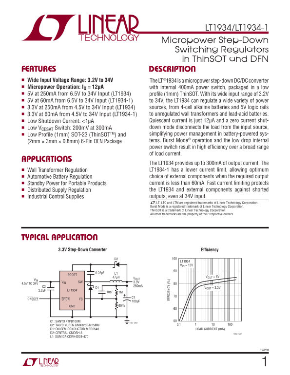
TYPICAL APPLICATION

3.3V Step-Down Converter Effi ciency

LT1934 VIN = 12V

BOOST

47μH VOUT = 5V

VIN SW 3.3V

4.5V TO 34V

D1 VOUT = 3.3V

2.2μF LT1934

ON OFF SHDN FB

100μF GND 604k

C1: SANYO 4TPB100M

1934 TA01

C2: TAIYO YUDEN GMK325BJ225MN 0.1

D1: ON SEMICONDUCTOR MBR0540 LOAD CURRENT (m A) D2: CENTRAL CMDSH-3 1934 TA02 L1: SUMIDA CDRH4D28-470

1934fd

Page Summary Contents For LINEAR TECHNOLOGY LT1934 LT1934-1 User's Manual

Page 1 LT1934/LT1934-1 Micropower Step-Down Switching Regulators in Thin SOT and DFN FEATURES DESCRIPTION n Wide Input Voltage Range: 3.2V to 34V The LT®1934 is a micropower step-down DC/DC converter n Micro...
Page 2 LT1934/LT1934-1 ABSOLUTE MAXIMUM RATINGS (Note 1) Input Voltage (VIN) ................................................... 34V Operating Temperature Range (Note 2) BOOST Pin Voltage ......................
Page 3 LT1934/LT1934-1 ELECTRICAL CHARACTERISTICS The ● denotes specifi cations which apply over the full operating temperature range, otherwise specifi cations are at TA = 25°C. VIN = 10V, VBOOST = 15V, unl...
Page 4 SW IT CH FF IM (μ s) FF IC IE FF IC IE LT1934/LT1934-1 TYPICAL PERFORMANCE CHARACTERISTICS LT1934 Effi ciency, VOUT = 5V LT1934 Effi ciency, VOUT = 3.3V LT1934-1 Effi ciency, VOUT = 5V LT1934 LT1934 L...
Page 5 LT1934/LT1934-1 TYPICAL PERFORMANCE CHARACTERISTICS Quiescent Current Undervoltage Lockout Minimum Input Voltage vs Temperature vs Temperature VOUT = 3.3V 4.0 6.0 LT1934 VOUT = 3.3V 5.5 TA = 25°C BOOS...
Page 6 LT1934/LT1934-1 BLOCK DIAGRAM BOOST ON TIME 12μs DELAY C3 OFF TIME 1.8μs DELAY ON OFF VREF 1.25V ENABLE FEEDBACK COMPARATOR GND FB 1934 BD 1934fd
Page 7 LT1934/LT1934-1 OPERATION (Refer to Block Diagram) The LT1934 uses Burst Mode control, combining both low fl ip-fl op when this current reaches 400m A (120m A for quiescent current operation and high ...
Page 8 LT1934/LT1934-1 APPLICATIONS INFORMATION Which One to Use: LT1934 or LT1934-1? The duty cycle is the fraction of time that the internal switch is on and is determined by the input and output The only ...
Page 9 LT1934/LT1934-1 APPLICATIONS INFORMATION Table 2. Inductor Vendors VENDOR PHONE URL PART SERIES COMMENTS Murata (404) 426-1300 www.murata.com LQH3C Small, Low Cost, 2mm Height Sumida (847) 956-0666 ww...
Page 10 LT1934/LT1934-1 APPLICATIONS INFORMATION capacitor is subject to large surge currents if the LT1934 The LT1934-1, with its lower switch current, can use a circuit is connected to a low impedance suppl...
Page 11 LT1934/LT1934-1 APPLICATIONS INFORMATION when used with ceramic capacitors will be lower and may D2 be acceptable. BOOST C3 A fi nal precaution regarding ceramic capacitors concerns LT1934 the maximum...
Page 12 LT1934/LT1934-1 IN IN APPLICATIONS INFORMATION Minimum Input Voltage VOUT = 3.3V to VIN), then the LT1934’s internal circuitry will pull its 6.0 quiescent current through its SW pin. This is fi ne if ...
Page 13 LT1934/LT1934-1 APPLICATIONS INFORMATION VIN SW VIN SW GND GND IC1 VSW VIN L1SW Figure 5. Subtracting the Current When the Switch is On (a) from the Current When the Switch is Off (b) Reveals the Path...
Page 14 LT1934/LT1934-1 APPLICATIONS INFORMATION Figure 7 shows the waveforms that result when an LT1934 an aluminum electrolytic capacitor has been added. This circuit is connected to a 24V supply through si...
Page 15 LT1934/LT1934-1 APPLICATIONS INFORMATION in series with the input to eliminate the voltage overshoot estimated by calculating the total power loss from an (it also reduces the peak input current). A 0...
Page 16 LT1934/LT1934-1 TYPICAL APPLICATIONS 3.3V Step-Down Converter BOOST 100μH VOUT VIN SW 3.3V 4.5V TO 34V 1μF LT1934-1 ON OFF SHDN FB GND 604k C1: TAIYO YUDEN JMK316BJ226ML 1934 TA04 C2: TAIYO YUDEN GMK3...
Page 17 LT1934/LT1934-1 TYPICAL APPLICATIONS 1.8V Step-Down Converter BOOST 33μH VOUT VIN SW 1.8V 3.6V TO 16V 2.2μF LT1934 ON OFF SHDN FB GND 332k C1: SANYO 2R5TPB100M 1934 TA06 C2: TAIYO YUDEN EMK316BJ225ML ...
Page 18 LT1934/LT1934-1 TYPICAL APPLICATIONS Standalone 350m A Li-Ion Battery Charger BOOST VIN 0.047μF VIN SW 7V TO 28V CHRG GATE LT1934 D1 1M LTC4052 ACPR SENSE 1μF SHDN FB GND C1 350m A 47μF GNDTIMER 1-CEL...
Page 19 LT1934/LT1934-1 PACKAGE DESCRIPTION S6 Package 6-Lead Plastic TSOT-23 (Reference LTC DWG # 05-08-1636) 2.90 BSC (NOTE 4) MAX REF 1.22 REF 2.80 BSC 3.85 MAX 1.4 MIN2.62 REF (NOTE 4) PIN ONE ID RECOMMEN...
Page 20 LT1934/LT1934-1 TYPICAL APPLICATION 5V Step-Down Converter BOOST VIN SW 5V 6.5V TO 34V 2.2μF LT1934 ON OFF SHDN FB 68μF GND 332k C1: SANYO 6TPB68M 1934 TA03 C2: TAIYO YUDEN GMK325BJ225MN D1: ZETEX ZHC...